
Superior system-on-chip designs are extraordinarily advanced by way of transistor rely and are arduous to construct utilizing the most recent fabrication processes. In a bid to make manufacturing of next-generation chips economically possible, chip fabs want to make sure excessive yields early of their lifecycle by rapidly discovering and correcting defects.
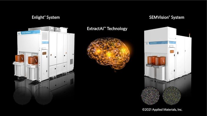
However discovering and fixing defects isn’t straightforward at the moment, as conventional optical inspection instruments do not provide sufficiently detailed picture decision, whereas high-resolution e-beam and multibeam inspection instruments are comparatively gradual. Trying to bridge the hole on inspection prices and time, Utilized Supplies has been growing a know-how known as ExtractAI know-how, which makes use of a mixture of the corporate’s newest Enlight optical inspection software, SEMVision G6/G7 e-beam assessment system, and deep studying (AI) to rapidly discover flaws. And surprisingly, this resolution has been in use for a couple of yr now.
UPDATE 3/21: Utilized Supplies despatched in an e mail to make clear that Extract AI can work not solely with the SEMVision G7, but additionally with the SEMVision G6.
“Utilized’s new playbook for course of management combines Large Information and AI to ship an clever and adaptive resolution that accelerates our clients’ time to most yield,” mentioned Keith Wells, group vp and basic supervisor, Imaging and Course of Management at Utilized Supplies. “By combining our best-in-class optical inspection and eBeam assessment applied sciences, we’ve created the business’s solely resolution with the intelligence to not solely detect and classify yield-critical defects but additionally study and adapt to course of modifications in real-time. This distinctive functionality allows chipmakers to ramp new course of nodes sooner and keep excessive seize charges of yield-critical defects over the lifetime of the method.”
Defect Detection: A Essential Step in Chip Manufacturing
As a extremely aggressive business, the semiconductor business can also be extraordinarily time delicate. Fashionable firms should develop new chips, bug repair them, after which launch all of them on pretty tight schedules. These days it takes years to develop a complicated chip and a number of other months to truly fabricate a batch. Probably the most essential time parameters is time to yield, which is to say with the ability to present numerous chips with excessive sufficient yields. A chip designer might have probably the most environment friendly structure round, but when they can not get it made in excessive volumes, they’re going to nonetheless lose out on cash and market share. Even foundries really feel this pinch, because the time wanted to repair defects and convey traces as much as snuff represents hundreds of thousands of {dollars} in gear depreciation alone – one week of a 3nm fab downtime is anticipated to price $25 million in unamortized depreciation prices. So reaching acceptable time to yield metrics closely will depend on a fab’s skill to detect and repair yield-killing defects.

For the reason that majority of superior SoCs are made utilizing extraordinarily small fabrication processes – lots of which depend on multi patterning and/or excessive ultraviolet (EUV) lithography – it’s getting very powerful to detect defects. Utilized Supplies says that the variety of course of steps elevated by 48% from 2015 to 2021.
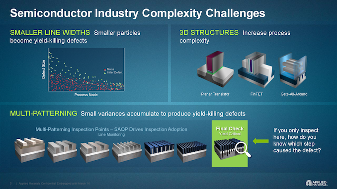
In the meantime, small variances and line widths can find yourself as yield-killing defects in the event that they multiply. Moreover, if these tiny variances are detected late, all the method steps made after the variance was launched are primarily wasted money and time. In truth, even late detection will be thought-about dangerous luck, as monitoring down the foundation reason behind a defect of an IC that includes FinFET transistors and made utilizing multi patterning is extraordinarily arduous.
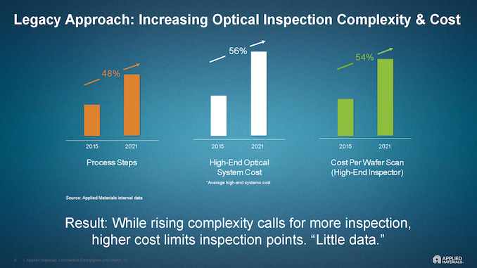
Identical to scanners used to construct chips, inspection instruments have advanced considerably through the years. However additionally they have turn into dearer, which will increase price per wafer scan. In line with Utilized Supplies, the worth tag on a high-end optical inspection system has elevated by 56% within the final six years, which in flip has elevated the associated fee per wafer scan by 54% in the identical interval.
Because of this, the fab business faces a catch-22. On the one hand, it must do extra inspections (ideally after every course of step) with a view to velocity up time to yield and make manufacturing extra environment friendly. Moreover, chipmakers are at all times performing steady course of enhancements (CPI), to enhance yields and scale back efficiency/energy variations utilizing statistical course of management (SPI), which once more includes extra inspections. However then again, since there are such a lot of course of steps at the moment and the inspection instruments are so costly, engineers should restrict inspection steps to maintain their course of management budgets from skyrocketing, which primarily stretches out the time to yield and whereas slowing down the CPI course of.
One more drawback confronted by fab engineers is the quantity of noise that’s captured by fashionable optical inspection instruments. In some unspecified time in the future noise turns into indistinguishable from yield-killing defects, so engineers have to use sure filtering fashions to cut back datasets they should work with. Fairly naturally, this reduces their skill to detect a defect early sufficient.
Utilizing AI for Wafer Inspection
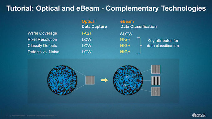
This brings us to Utilized Supplies’ ExtractAI know-how. As one of many world’s largest manufacturing software producers, Utilized Supplies has their hand in a broad vary of inspection instruments, together with optical inspection instruments and e-beam assessment instruments. So the corporate is trying to faucet its experience within the discipline to discover a approach to make use of each applied sciences to mitigate every software’s respect drawbacks – fast-but-resolution-limited optical inspection instruments, and slow-but-detailed e-beam instruments.

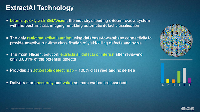
To that finish, Utilized Supplies has mixed its newest Enlight optical wafer inspection system with their new ExtractAI know-how. The ExtractAI software program primarily makes use of deep studying (AI) to attempt to higher interpret the outcomes of optical scanners, processing the optical information whereas utilizing their SEMVision G6/G7 e-beam assessment system as a supply of coaching and outcomes verification.
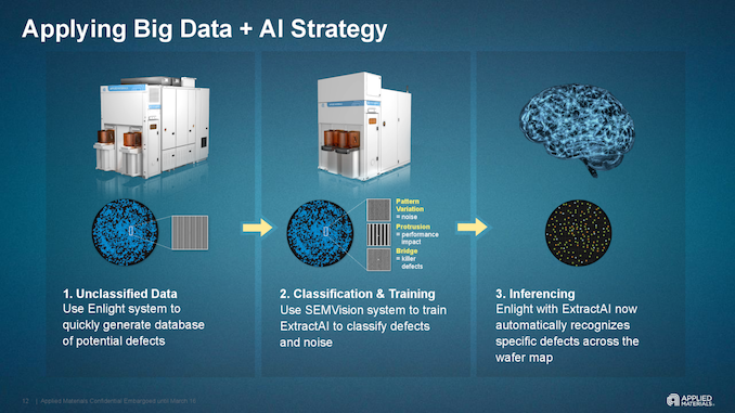

On paper, all the things works fairly simple. An Enlight system captures a high-resolution picture of a wafer and rapidly generates database of potential defects. The wafer is then despatched to a SEMVision G6/G7 e-beam assessment system that distinguishes defects from noise and classifies defects. Photos and information captured by the Enlight and the SEMVision G6/G7 are then fed to the ExtractAI software program to coach it to routinely acknowledge particular yield-killing defects throughout the wafer map generated utilizing the {hardware} programs and distinguish them from noise.
Because of this, the scanning course of takes significantly much less time with future wafers of the identical chip, because the programs have already got an actionable wafer map with potential yield-killing defects and will know what to search for. In the meantime, because the ExtractAI software program features extra information from extra wafers, the extra coaching ought to permit it to supply much more accuracy and efficiency. Particularly because the ensuing defect databases will be shared throughout a fab and even throughout the entire firm.
Already at Work
Because it often occurs with Utilized Supplies’ bulletins, their latest toolset is already put in at a number of fabs. In line with the corporate, their Enlight optical inspection software with ExtractAI know-how is already in use at logic fabs in South Korea, Taiwan, and the U.S., all of whom are utilizing it to enhance the time to yield of their newest applied sciences.
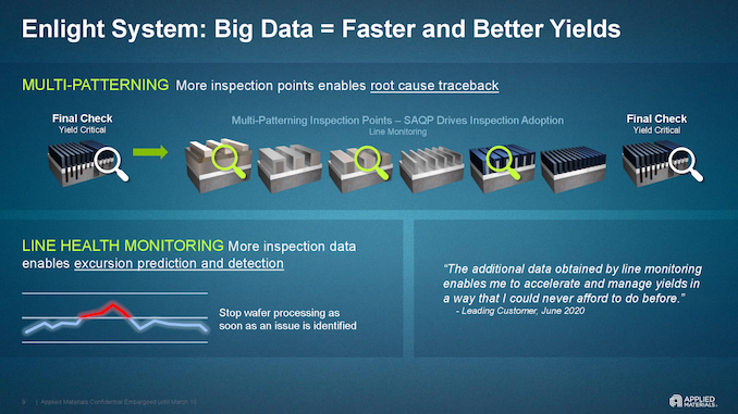
“The extra information obtained by line monitoring allows me to speed up and handle yields in a approach that I may by no means afford to do earlier than,” mentioned an unnamed buyer of Utilized in June 2020 (in keeping with the corporate’s presentation).
Utilized Supplies began improvement of the Enlight system with ExtractAI in 2016, with business shipments to logic producers starting in Q1 2020. By the top of Q1 2021, cumulative gross sales of the inspection software are anticipated to exceed $400 million. Utilized’s SEMVision e-beam inspection instruments are additionally broadly utilized by the business (over 1,500 models have been put in since 1998), however solely the SEMVision G6, G7 and their successors are appropriate with the Enlight and ExtractAI.
Right this moment, Utilized Supplies’ Enlight optical inspection system with ExtractAI know-how are being utilized by main logic fabs (since there are usually not lots of them, their names are usually not arduous to guess). However as DRAM course of applied sciences proceed to get extra advanced, the corporate is anticipating that producers in different fab fields will undertake Utilized’s deep learning-driven toolset within the coming quarters and years as properly.


