
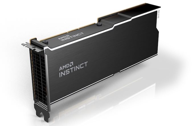
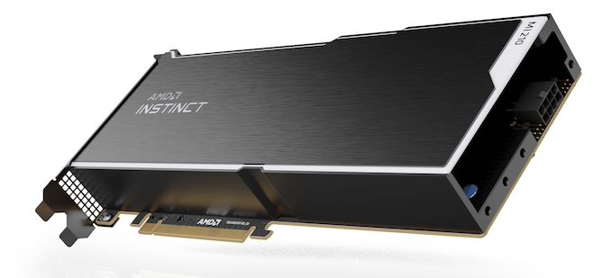
With each GDC and GTC occurring this week, this can be a large time for GPUs of all types. And as we speak, AMD desires to get in on the sport as effectively, with the discharge of the PCIe model of their MI200 accelerator household, the MI210.
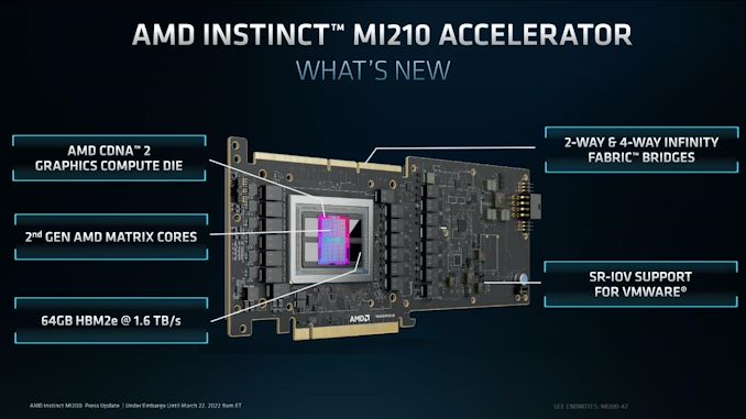
First unveiled alongside the MI250 and MI250X again in November, when AMD initially launched the Intuition MI200 household, the MI210 is the third and remaining member of AMD’s newest technology of GPU-based accelerators. Bringing the CDNA 2 structure right into a PCIe card, the MI210 is being geared toward prospects who’re after the MI200 household’s HPC and machine studying efficiency, however want it in a standardized kind issue for mainstream servers. Total, the MI200 is being launched extensively as we speak as a part of AMD transferring the whole MI200 product stack to normal availability for OEM prospects.
| AMD Intuition Accelerators | ||||||
| MI250 | MI210 | MI100 | MI50 | |||
| Compute Items | 2 x 10⁴ | 104 | 120 | 60 | ||
| Matrix Cores | 2 x 416 | 416 | 480 | N/A | ||
| Enhance Clock | 1700MHz | 1700MHz | 1502MHz | 1725MHz | ||
| FP64 Vector | 45.3 TFLOPS | 22.6 TFLOPS | 11.5 TFLOPS | 6.6 TFLOPS | ||
| FP32 Vector | 45.3 TFLOPS | 22.6 TFLOPS | 23.1 TFLOPS | 13.3 TFLOPS | ||
| FP64 Matrix | 90.5 TFLOPS | 45.3 TFLOPS | 11.5 TFLOPS | 6.6 TFLOPS | ||
| FP32 Matrix | 90.5 TFLOPS | 45.3 TFLOPS | 46.1 TFLOPS | 13.3 TFLOPS | ||
| FP16 Matrix | 362 TFLOPS | 181 TFLOPS | 184.6 TFLOPS | 26.5 TFLOPS | ||
| INT8 Matrix | 362.1 TOPS | 181 TOPS | 184.6 TOPS | N/A | ||
| Reminiscence Clock | 3.2 Gbps HBM2E | 3.2 Gbps HBM2E | 2.4 Gbps HBM2 | 2.0 Gbps GDDR6 | ||
| Reminiscence Bus Width | 8192-bit | 4096-bit | 4096-bit | 4096-bit | ||
| Reminiscence Bandwidth | 3.2TBps | 1.6TBps | 1.23TBps | 1.02TBps | ||
| VRAM | 128GB | 64GB | 32GB | 16GB | ||
| ECC | Sure (Full) | Sure (Full) | Sure (Full) | Sure (Full) | ||
| Infinity Cloth Hyperlinks | 6 | 3 | 3 | N/A | ||
| CPU Coherency | No | N/A | N/A | N/A | ||
| TDP | 560W | 300W | 300W | 300W | ||
| Manufacturing Course of | TSMC N6 | TSMC N6 | TSMC 7nm | TSMC 7nm | ||
| Transistor Depend | 2 x 29.1B | 29.1B | 25.6B | 13.2B | ||
| Structure | CDNA 2 | CDNA 2 | CDNA (1) | Vega | ||
| GPU | 2 x CDNA 2 GCD “Aldebaran” |
CDNA 2 GCD “Aldebaran” |
CDNA 1 “Arcturus” |
Vega 20 | ||
| Kind Issue | OAM | PCIe (4.0) | PCIe (4.0) | PCIe (4.0) | ||
| Launch Date | 11/2021 | 03/2022 | 11/2020 | 11/2018 | ||
Beginning with a take a look at the top-line specs, the MI210 is an fascinating variant to the prevailing MI250 accelerators. Whereas these two elements had been primarily based on a pair of Aldebaran (CDNA 2) dies in an MCM configuration on a single package deal, for MI210 AMD is paring all the things again to a single die and associated {hardware}. With MI250(X) requiring 560W within the OAM kind issue, AMD primarily wanted to halve the {hardware} anyhow to get issues right down to 300W for a PCIe card. So that they’ve completed so by ditching the second on-package die.
The online result’s that the MI210 is basically half of an MI250, each with reference to bodily {hardware} and anticipated efficiency. The CNDA 2 Graphics Compute Die options the identical 104 enabled CUs as on MI250, with the chip operating on the identical peak clockspeed of 1.7GHz. So workload scalability apart, the efficiency of the MI210 is for all sensible functions half of a MI250.
That halving goes for reminiscence, as effectively. As MI250 paired 64GB of HBM2e reminiscence with every GCD – for a complete of 128GB of reminiscence – MI210 brings that right down to 64GB for the one GCD. AMD is utilizing the identical 3.2GHz HBM2e reminiscence right here, so the general reminiscence bandwidth for the chip is 1.6 TB/second.
With reference to efficiency, using a single Aldebaran die does make for some odd comparisons to AMD’s previous-generation PCIe card, the Radeon Intuition MI100. Whereas clocked increased, the marginally diminished variety of CUs relative to the MI100 signifies that for some workloads, the previous accelerator is, at the very least on paper, a bit quicker. In follow, MI210 has extra reminiscence and extra reminiscence bandwidth, so it ought to nonetheless have the efficiency edge the actual world, however it’s going to be shut. In workloads that may’t benefit from CDNA 2’s architectural enhancements, MI210 shouldn’t be going to be a step up from MI100.
All of this underscores the general similarity between the CDNA (1) and CDNA 2 architectures, and the way builders must make use of CDNA 2’s new options to get essentially the most out of the {hardware}. The place CDNA 2 shines compared to CDNA (1) is with FP64 vector workloads, FP64 matrix workloads, and packed FP32 vector workloads. All three use circumstances profit from AMD doubling the width of their ALUs to a full 64-bits huge, permitting FP64 operations to be processed at full pace. In the meantime, when FP32 operations are packed collectively to fully fill the broader ALU, then they can also profit from the brand new ALUs.
However, as we famous in our preliminary MI250 dialogue, like all packed instruction codecs, packed FP32 isn’t free. Builders and libraries should be coded to benefit from it; packed operands should be adjoining and aligned to even registers. For software program being written particularly for the structure (e.g. Frontier), that is simply sufficient completed, however extra moveable software program will want up to date to take this under consideration. And it’s for that motive that AMD properly nonetheless advertises its FP32 vector efficiency at full charge (22.6 TFLOPS), moderately than assuming using packed directions.
The launch of the MI210 additionally marks the introduction of AMD’s improved matrix cores right into a PCIe card. For CDNA 2, they’ve been expanded to permit full-speed FP64 matrix operation, bringing them as much as the identical 256 FLOPS charge as FP32 matrix operations, a 4x enchancment over the previous 64 FLOPS/clock/CU charge.
| AMD GPU Throughput Charges (FLOPS/clock/CU) |
|||||
| CDNA 2 | CDNA (1) | Vega 20 | |||
| FP64 Vector | 128 | 64 | 64 | ||
| FP32 Vector | 128 | 128 | 128 | ||
| Packed FP32 Vector | 256 | N/A | N/A | ||
| FP64 Matrix | 256 | 64 | 64 | ||
| FP32 Matrix | 256 | 256 | 128 | ||
| FP16 Matrix | 1024 | 1024 | 256 | ||
| BF16 Matrix | 1024 | 512 | N/A | ||
| INT8 Matrix | 1024 | 1024 | N/A | ||
Transferring on, the PCIe format MI210 additionally will get a trio of Infinity Cloth 3.0 hyperlinks alongside the highest of the cardboard, identical to the MI100. This permits an MI210 card to be linked up with one or three different playing cards, forming a 2 or 4-way cluster of playing cards. In the meantime, backhaul to the CPU or every other PCIe gadgets is supplied through a PCIe 4.0 x16 connection, which is being powered by one of many versatile IF hyperlinks from the GCD.
As beforehand talked about, the TDP for the MI210 is ready at 300W, the identical degree because the MI100 and MI50 earlier than it – and primarily the restrict for a PCIe server card. Like most server accelerators, that is absolutely passive twin slot card design, counting on vital airflow from the server chassis to maintain issues cool. The GPU itself is powered by a mixture of the PCIe slot and an 8 pin, EPS12V connector on the rear of the cardboard.
In any other case, regardless of the change in kind components, AMD goes after a lot the identical market with MI210 as they’ve MI250(X). Which is to say HPC customers who particularly want a quick FP64 accelerator. Due to its heritage as a chip designed at the start for supercomputers (i.e. Frontier), the MI200 household presently stands alone in its FP64 vector and FP64 matrix efficiency, as rival GPUs have centered as an alternative on enhancing efficiency on the decrease precisions utilized in most business/non-scientific workloads. Although even at decrease precisions, the MI200 household is nothing to sneeze at with tis 1024 FLOPS-per-CU charge on FP16 and BF16 matrix operations.
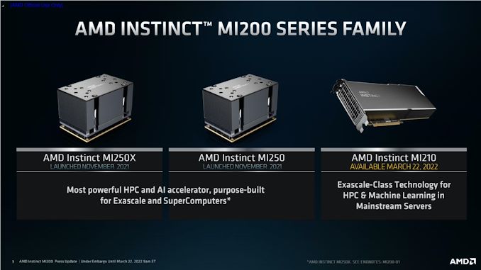
Wrapping issues up, MI210 is slated to turn out to be accessible as we speak from AMD’s common server companions, together with ASUS, Dell, Supermicro, HPE, and Lenovo. These distributors at the moment are additionally providing servers primarily based on AMD’s MI250(X) accelerators, so AMD’s extra mainstream prospects can have entry to programs primarily based on AMD’s full lineup of MI200 accelerators.


