
With AMD’s first-wave of Zen 4 CPUs now within the books with the Ryzen 7000 sequence, the patron arm of AMD is now shifting its consideration over to its graphics enterprise. In a presentation that ended moments in the past dubbed “collectively we advance_gaming”, Dr. Lisa Su and different AMD leaders laid out the way forward for AMD’s graphics merchandise. And that future is the RDNA 3 structure, which would be the foundation of the brand new Radeon RX 7900 XTX and Radeon RX 7900 XT video playing cards.
The 2 playing cards, set to be launched on December 13th, would be the first merchandise launched utilizing the RDNA 3 structure. In keeping with AMD, the brand new flagship 7900 XTX will ship as much as 70% extra efficiency at 4K than their earlier flagship, the 6950 XT. This efficiency increase comes curtesy of a number of architectural enhancements in RDNA that cumulatively provide 54% larger efficiency per watt than RDNA 2, in addition to larger clockspeeds courtesy of TSMC’s 5nm (and 6nm) processes, and better general energy consumption.
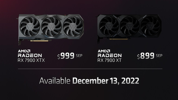
The complete-fledged RX 7900 XTX might be hitting the streets at $999. In the meantime the second-tier RX 7900 XT will run for $899.
| AMD Radeon RX 7000 Sequence Specification Comparability | ||||||
| AMD Radeon RX 7900 XTX | AMD Radeon RX 7900 XT | AMD Radeon RX 6950 XT | AMD Radeon RX 6900 XT | |||
| Stream Processors | 12288 (96 CUs) |
10752 (84 CUs) |
5120 (80 CUs) |
5120 (80 CUs) |
||
| ROPs | ? | ? | 128 | 128 | ||
| Sport Clock | 2.3GHz | 2.0GHz | 2100MHz | 2015MHz | ||
| Enhance Clock | ~2.5GHz | ? | 2310MHz | 2250MHz | ||
| Throughput (FP32) | 56.5 TFLOPS | 43 TFLOPS | 21.5 TFLOPS | 20.6 TFLOPS | ||
| Reminiscence Clock | 20 Gbps GDDR6 | 20 Gbps GDDR6 | 18 Gbps GDDR6 | 16 Gbps GDDR6 | ||
| Reminiscence Bus Width | 384-bit | 320-bit | 256-bit | 256-bit | ||
| VRAM | 24GB | 20GB | 16GB | 16GB | ||
| Infinity Cache | 96MB | 80MB | 128MB | 128MB | ||
| Whole Board Energy | 355W | 300W | 335W | 300W | ||
| Manufacturing Course of | GCD: TSMC 5nm MCD: TSMC 6nm |
GCD: TSMC 5nm MCD: TSMC 6nm |
TSMC 7nm | TSMC 7nm | ||
| Transistor Rely | 58B | 58B – (1 MCD) | 26.8B | 26.8B | ||
| Structure | RDNA3 | RDNA3 | RDNA2 | RDNA2 | ||
| GPU | Massive Navi 3x | Massive Navi 3x | Navi 21 | Navi 21 | ||
| Launch Date | 12/13/2022 | 12/13/2022 | 05/10/2022 | 12/08/2020 | ||
| Launch Worth | $999 | $899 | $1099 | $999 | ||
AMD’s eagerly anticipated replace to their GPU structure comes as the corporate has been firing on all cylinders for the previous few years. On the CPU aspect of issues the Zen 3 and Zen 4 architectures particularly have confirmed very performant, and in the meantime AMD has been capable of claw its means again from its graphics stoop with the RDNA household of GPU architectures. RDNA 2, the premise of the Radeon RX 6000 sequence, exceeded expectations and proved to be a really sturdy competitor, and now AMD is seemingly setup to exceed expectations as soon as once more, with RDNA 3’s 54% performance-per-watt coming in forward of AMD’s earliest guarantees of a 50% acquire.
AMD Goes Chiplets For GPUs
Whereas as we speak’s reveal from AMD was a extra intently guarded occasion than the Ryzen 7000 unveil a few months in the past, AMD has nonetheless given us a fairly a little bit of element on the RDNA 3 structure and the playing cards – greater than we’ve got time to cowl right here – so let’s get began from the highest, with the development of the primary RDNA 3 GPU.
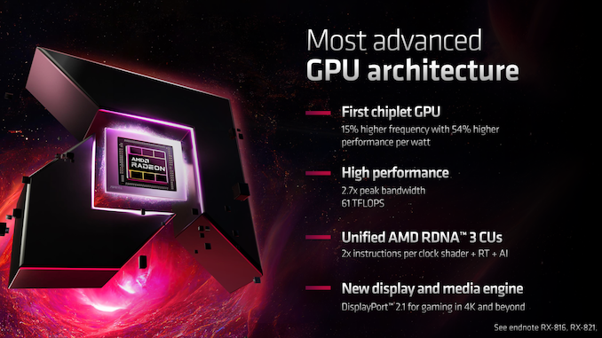
The Navi 3x GPU (AMD will not be confirming the particular GPU identify at the moment) breaks new floor for AMD not solely on the efficiency entrance, however when it comes to its development. For the primary time from any of the massive 3 GPU producers, AMD is using chiplets within the development of the GPU.
Chiplets are in some respects the holy grail of GPU development, as a result of they provide GPU designers choices for breaking up advanced monolithic GPU designs into a number of smaller components – permitting for brand new choices for scaling, in addition to mixing and matching the method node utilized in manufacturing. That stated, it’s additionally a holy grail as a result of the immense quantity of information that have to be handed between completely different components of a GPU (on the order of terabytes per second) could be very arduous to do – and really essential to do in order for you a multi-chip GPU to have the ability to current itself as a single system.
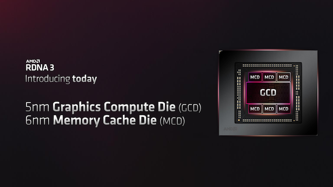
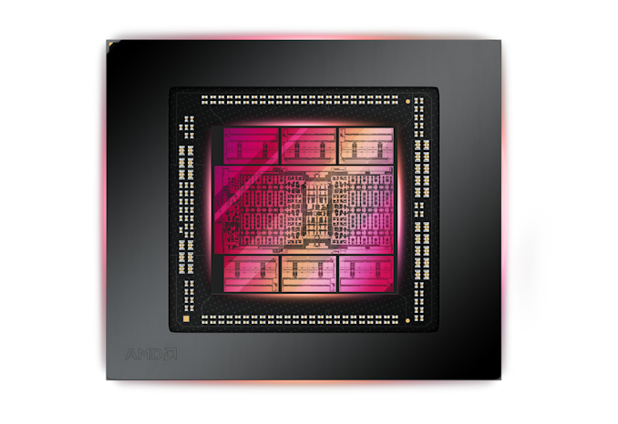
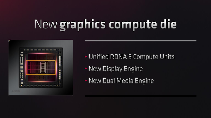
For his or her huge Navi 3x chip, AMD has assembled two varieties of chiplets, primarily breaking off the reminiscence capabilities from a traditional GPU into their very own chiplets. Because of this the core capabilities of the GPU are housed in what AMD is looking the Graphics Compute Die (GCD), which homes the entire ALU/compute {hardware}, the graphics {hardware}, in addition to ancillary blocks just like the show and media engines.
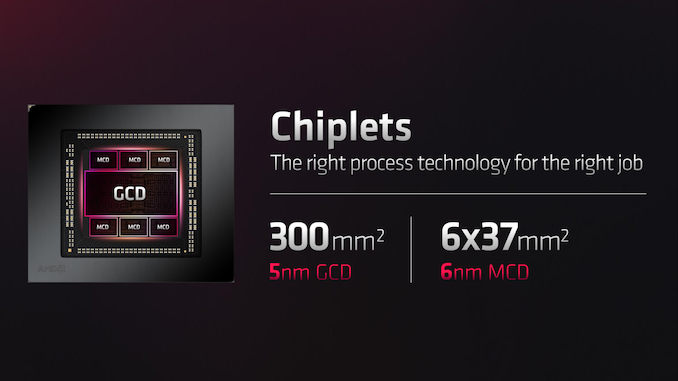
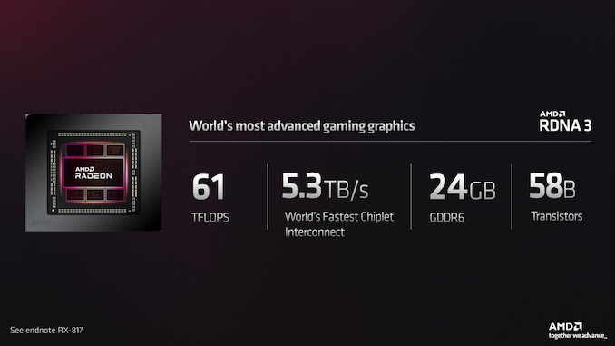
As a result of the GCD homes the performance-critical points of the general GPU, it’s being constructed on TSMC’s 5nm course of. This offers AMD one of the best density, energy consumption, and clockspeeds for these components, although clearly at a better manufacturing price. The GCD die dimension measures 300mm2.
In the meantime the brand new Reminiscence Cache Die (MCD) homes AMD’s infinity cache (L3 cache), in addition to a 64-bit (technically 2×32-bit) GDDR6 reminiscence controllers. The MCD is without doubt one of the scalable points of the chiplet design, as Massive Navi 3x GPU SKUs may be configured by paring them with extra or fewer MCDs. A full configuration on this case is 6 energetic MCDs, which is what we see within the 7900 XTX. In the meantime the 7900 XT could have 5 energetic MCDs, with a 6th faulty/spacer MCD current for salvaging functions and bodily bundle stability.
A person MCD is 37mm2 in die dimension, and is constructed on TSMC’s 6nm course of. That is an instance of AMD’s course of node flexibility, placing the much less essential GDDR6 reminiscence controllers and Infinity Cache on a less expensive course of node. GDDR6 controllers are a type of traditional examples of a know-how that doesn’t scale very properly with smaller course of geometries (like most types of I/O), so it’s simple to see why AMD would need to keep away from constructing it on 5nm for minimal advantages.
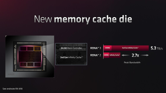
Within the full 6 MCD configuration (7900 XTX), Massive Navi 3x gives a 384-bit GDDR6 reminiscence bus, together with 96MB of L3 cache. In the meantime a 5 MCD (7900 XT) gives a 320-bit GDDR6 reminiscence bus and 80MB of L3 cache.
For the needs of as we speak’s announcement, AMD has not gone into nice depth on how they managed to make a chiplet-based GPU work, however they’ve confirmed a couple of necessary particulars. Before everything, to be able to provide the die-to-die bandwidth wanted have the reminiscence subsystem situated off-chip, AMD is utilizing their Elevated Fanout Bridge (EFB) packaging know-how, which AMD first used for his or her Intuition MI200 sequence accelerators (CDNA2). On these accelerator components it was used to hook up the monolithic GPUs to one another, in addition to HBM2e reminiscence. On RDNA 3, it’s getting used to hook up the MCDs to the GCD.
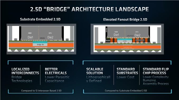
Notably, Elevated Fanout Bridge is a non-organic packaging know-how, which is to say it’s advanced. That AMD is ready to get 5.3TB/second of die-to-die bandwidth by way of it underscores its utility, nevertheless it additionally implies that AMD is undoubtedly paying a superb deal extra for packaging on Massive Navi 3x than they had been on Navi 21 (or Ryzen 7000).
Internally, AMD is looking this memory-to-graphics hyperlink Infinity Hyperlink. Which, because the identify implies, is chargeable for (transparently) routing AMD’s Infinity Cloth between dies.
As talked about earlier than, the cumulative bandwidth right here between the MCDs and GCD is 5.3TB/second. It’s unclear if the constraining issue is the bandwidth of the Infinity Hyperlink, or that the mixed Infinity Cache + GDDR6 reminiscence controllers can not transfer sufficient information to completely saturate the hyperlink. However regardless, it means there’s primarily simply shy of 900GB/second of bandwidth between a person MCD and GCD – greater than the entire mixed off-die reminiscence bandwidth of the last-generation Radeon RX 6950 XT (and a couple of.7x greater than Navi 21’s on-die bandwidth).
Whereas we’re with regards to AMD’s L3 Infinity Cache, it’s notable right here that it’s truly a bit smaller on Massive Navi 3x than it was on Navi 21, with a most capability of 96MB versus 128MB on the previous. In keeping with AMD they’ve made additional enhancements to enhance information reuse on the Infinity Cache to offset this drop in capability. At this level it’s not clear if the change is a operate of software program algorithms, or in the event that they’ve made extra elementary {hardware} modifications.
Lastly, whereas AMD is quoting die sizes for the GCD and MCD, they aren’t quoting particular person transistor counts. So whereas we all know {that a} full 6 MCD Massive Navi 3x configuration is comprised of 58 billion transistors (2.16x greater than Navi 21), we don’t know the way a lot of that’s the GCD versus the MCDs.
AMD RDNA 3 Compute & Graphics Structure: Bringing Again ILP & Bettering RT
Diving down a stage, let’s check out the precise graphics and compute structure backing RDNA 3 and Massive Navi 3x.
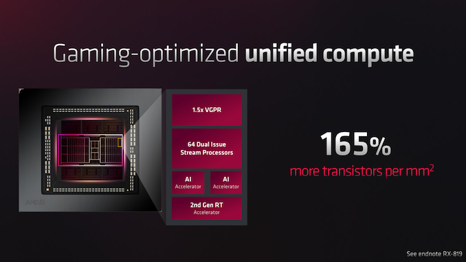
Whereas nonetheless clearly sharing lots of the core design components of AMD’s overarching RDNA structure, RDNA 3 is in some respects a a lot larger shift in architectural design than RDNA 2 was. Whereas RDNA 2’s compute core was primarily unchanged from RDNA (1)’s, RDNA 3 makes a couple of huge modifications.
The most important influence is how AMD is organizing their ALUs. Briefly, AMD has doubled the variety of ALUs (Stream Processors) inside a CU, going from 64 ALUs in a single Twin Compute Unit to 128 inside the identical unit. AMD is engaging in this not by doubling up on the Twin Compute Items, however as an alternative by giving the Twin Compute Items the power to dual-issue directions. Briefly, every SIMD lane can now execute as much as two directions per cycle.
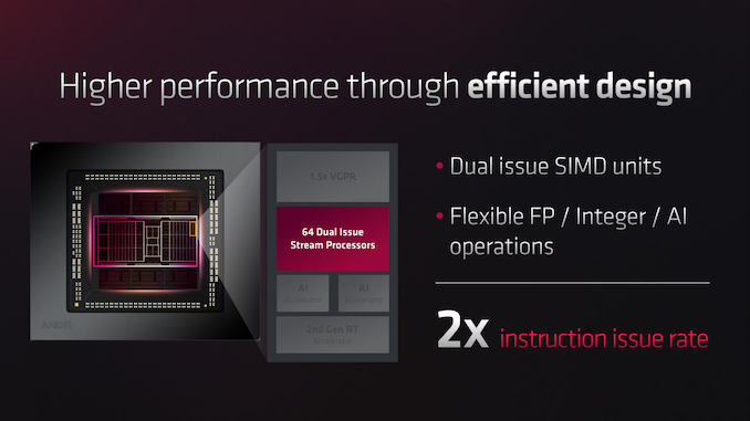
However, as with all dual-issue configurations, there’s a trade-off concerned. The SIMDs can solely subject a second instruction when AMD’s {hardware} and software program can extract a second instruction from the present wavefront. Because of this RDNA 3 is now explicitly reliant on extracting Instruction Stage Parallelism (ILP) from wavefronts to be able to hit most utilization. If the following instruction in a wavefront can’t be executed in parallel with the present instruction, then these further ALUs will go unfilled.
This can be a notable change as a result of AMD developed RDNA (1) partly to get away from a reliance on ILP, which was recognized as a weak point of GCN – which was why AMD’s real-world throughput was not as quick as their on-paper FLOPS numbers would indicated. So AMD has, in some respects, walked backwards on that change by re-introducing an ILP dependence.
We’re nonetheless ready on extra info from AMD outlining why they made this modification. However dual-issue is often an inexpensive means so as to add extra throughput to a processor design (you don’t need to do all of the instruction monitoring required for a totally separate Twin Compute Unit), and it may be worthwhile tradeoff should you can make sure you’ll be capable of dual-issue more often than not. However it implies that AMD’s real-world ALU utilization charge is probably going decrease on RDNA 3 than RDNA 2, as a result of bubbles from not having the ability to dual-issue.
Which to deliver issues again to gaming and the merchandise at hand, it implies that the FLOPS numbers between RDNA 3 and RDNA 2 components will not be going to be completely comparable. 7900 XTX could push 2.6x as many FP32 FLOPs as 6950 XTX on paper, however the true world benefit on something lower than ultimate code goes to be much less. Which is without doubt one of the explanation why AMD is barely selling a real-world efficiency uplift of 1.7x for the 7900 XTX.
In any case, SIMDs aren’t the one modifications to the core compute structure of RDNA 3. Feeding the beast, AMD has made the Vector Common Function Register (VGPR) financial institution 50% bigger than on RDNA 2.
Extra important than that’s that AMD is lastly integrating devoted silicon for AI processing on their shopper GPUs. That is an space the place each of AMD’s opponents (NVIDIA and Intel) have already made the funding on their shopper components, and as using GPU inference in workloads continues to develop, it’s not one thing AMD can ignore any longer.
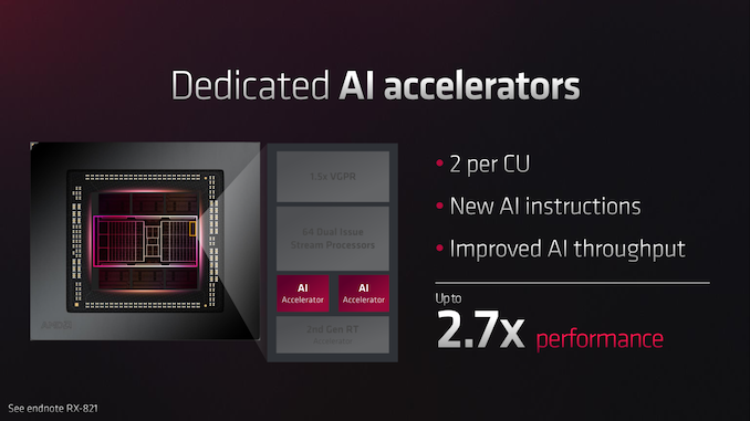
Given the gaming-centric focus of as we speak’s presentation, AMD didn’t spend a lot time speaking concerning the new AI items. Every RDNA 3 CU could have 2 of those items, and they’ll help new AI directions (some type of INT8 tensor operation looks like a given). All instructed, AMD is saying that the brand new AI items give the Radeon RX 7900 XTX 2.7x the AI efficiency, which AMD is measuring as bfloat16 efficiency versus the RX 6950 XT.
Total, the significance of this to players is one thing that is still to be seen. AMD isn’t at present utilizing AI items for FSR 2 (not like NVIDIA’s DLSS 2). However that would change for future tasks. In any other case, for extra skilled customers (or anybody who likes to mess with Secure Diffusion), that is an addition that’s excellent news.
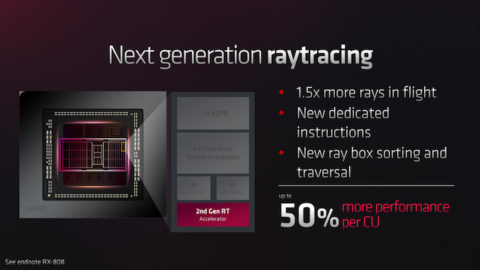
Transferring on, AMD has additionally up to date their raytracing {hardware} for RDNA 3. The second-generation RT accelerator, as AMD calls it, can deal with 1.5x extra rays in flight. There are additionally new {hardware} field sorting and traversal options that weren’t current in RDNA 2’s preliminary RT performance. AMD’s presentation gave the technical particulars a light-weight remedy, nevertheless it definitely appears to be like like AMD is transferring to doing a much bigger a part of the ray tracing course of in devoted {hardware}. Which in flip would assist enhance their efficiency, and hold efficiency steadier by not stealing fairly so many sources from the remainder of the CU.
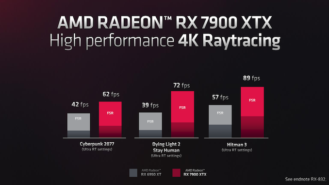
AMD’s personal efficiency slides tout anyplace between a 47% and 84% improve in RT efficiency. Although it needs to be famous that AMD’s numbers are with FSR enabled; so we can not divorce these positive aspects from any modifications that enhance FSR efficiency on the 7900 XTX.
Final, however not least, AMD has made an attention-grabbing resolution with clockspeeds on the RDNA 3. Briefly, AMD has decoupled their clocks; moderately than working the whole GCD on the identical clockspeed, AMD might be working the shaders and front-end at completely different clockspeeds. Within the case of the 7900 XTX, this may see the shaders working at 2.3GHz (the marketed sport clock pace), whereas the front-end will run at a barely speedier 2.5GHz (about 9% quicker).
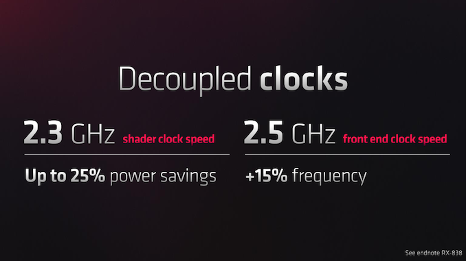
AMD didn’t go into nice element on why they’ve made this modification, however at a excessive stage it’s all about balancing efficiency versus energy consumption. The shaders might run at 2.5GHz as properly (certainly, the 7900 XTX’s rated increase clock is 2.5GHz), however as we’ve seen time and time once more, these closing clocks are the most costly when it comes to energy as you go up the v/f curve. So AMD has made the selection to surrender a little bit of potential efficiency to avoid wasting quite a bit on energy, as 96 CUs/12288 ALUs is a whole lot of silicon to gentle up. Conversely, the front-end is comparatively small, and with AMD having beefed up their CUs by a lot, spending a bit extra energy on the front-end is presumably value it to maintain them from bottlenecking the remainder of the GPU.
RDNA 3 Show & Media Engines: The Newest and the Biggest
AMD’s core compute/graphics structure was not the one a part of the RDNA 3 structure to get an replace on this era. AMD has additionally used the chance to improve their show and media engines to help new options and new codecs.
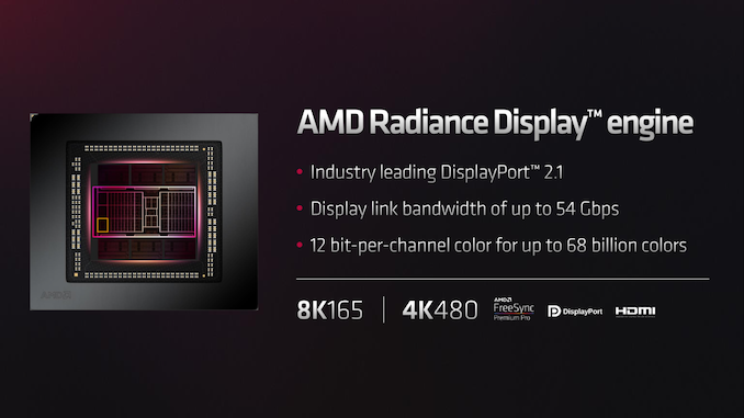
On the show engine entrance, AMD’s show engine, which they’re now calling the “AMD Radiance Show Engine” has been upgraded to help DisplayPort 2.1. Particularly, AMD has added help for the DisplayPort 2.x characteristic suite in addition to the UHBR 10 and UHBR 13.5 information charges. Because of this RDNA 3 playing cards can provide 2x the DisplayPort bandwidth of their DisplayPort 1.4-enabled predecessors, which in flip permits for larger resolutions and better refresh charges. Notably, this ever so barely exceeds HDMI 2.1’s bandwidth as properly, placing DisplayPort again into the lead, at the very least on AMD playing cards.
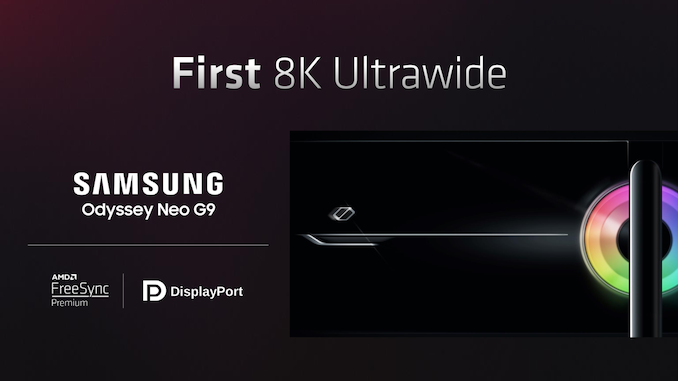
Unsurprisingly, AMD is utilizing this performance to push forthcoming larger decision and better refresh charge gaming displays, together with a Samsung ultrawide show set to launch in 2023 with a horizonal 8K decision. So it’s not only for displaying off specs, and AMD and its companions are intending to place it to good use.
AMD has not stated something concerning the whole variety of supported shows. So at this level I anticipate it’s nonetheless a most of 4 shows.
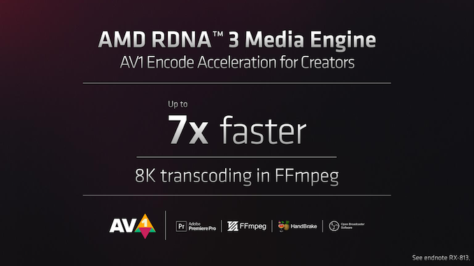
In the meantime on the media engine entrance, AMD has given RDNA 3 help for the newest and best video codecs. Together with the standard H.264 and H.265 help, RDNA 3’s media engines additionally add full AV1 encode and decode help, making this the newest GPU household to roll out help for the next-generation open format codec. RDNA 3 will be capable of encode and decode AV1 at as much as 8Kp60.
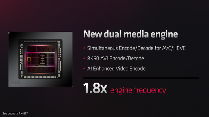
The general efficiency of the media engine has been elevated considerably. In keeping with AMD the media engine runs 80% quicker than it did on RDNA 2 components, permitting for simultaneous encoding (or decoding) of as much as two H.264/H.265 streams. Although it’s unclear if that additionally applies to AV1.
Lastly with regards to AMD’s GPU uncore, whereas not explicitly referred to as out in AMD’s presentation, it’s value noting that AMD has not up to date their PCIe controller. So RDNA 3 nonetheless maxes out at PCIe 4.0 speeds, with Massive Navi 3x providing the standard 16 lanes. Because of this regardless that AMD’s newest Ryzen platform helps PCIe 5.0 for graphics (and different PCIe playing cards), their video playing cards received’t be reciprocating on this era. Actually, because of this nobody could have a PCIe 5.0 shopper video card.
Radeon RX 7900 XTX & Radeon RX 7900 XT: Launching December 13th
Bringing as we speak’s reveal full circle, let’s flip again to the playing cards themselves, the Radeon RX 7900 XTX and RX 7900 XT.
AMD’s flagship card would be the Radeon RX 7900 XTX. Whereas we’re nonetheless ready on affirmation of this, this may appear to be a fully-enabled Massive Navi 3x half, with the entire blocks in each the GCDs and the person MCDs themselves enabled. As talked about beforehand, AMD is touting a broad efficiency uplift of as much as 70% versus the previous-generation flagship, the RX 6950 XT.
Internally, this implies 96CUs and 96MB of L3 Infinity Cache might be accessible on the cardboard. The sport clock (common clockspeed) might be 2.3GHz, whereas based mostly on different AMD figures, we are able to infer that the increase (most) clockspeed might be 2.5GHz. The sport clock particularly is a ~10% enchancment over the 6950 XT, so AMD is having fun with a modest frequency uplift generation-over-generation, however nothing too large. Many of the heavy lifting will come courtesy of the structure and reminiscence modifications.
Talking of reminiscence, the RX 7900 XTX might be paired with 24GB of GDDR6 reminiscence working at (at the very least) 20Gbps. Apparently, AMD’s companions have the headroom to go even larger than this with manufacturing facility overclocking, however the ground worth for the half might be 20Gbps general. This can be a modest improve in reminiscence clockspeeds versus the 6950 XT (11%). As an alternative, the majority of the VRAM bandwidth positive aspects will come from the 50% bigger reminiscence bus, with the 7900 XTX transferring to a large 384-bit bus. In whole, this implies the 7900 XTX could have 960GB/sec of reminiscence bandwidth, 66% greater than its predecessor. AMD bought their “free” reminiscence subsystem efficiency increase within the final era with Infinity Cache, so for this time round, they’re again to needing so as to add extra bodily reminiscence bandwidth to maintain the ever-growing beast correctly fed.
In the meantime, the 7900 XT might be a chip off the block, with fewer CUs, much less VRAM, and decrease clockspeeds. All instructed we’re 84CUs paired with 20GB of 20Gbps GDDR6, and backed by an 80MB infinity cache. The cardboard’s sport clockspeed ranking is 2.0GHz, and we shouldn’t have any info on the increase clockspeed. The mixture of a 13% drop in clockspeeds and 13% drop in CUs provides up to what’s, on paper, a 24% deficit in compute/shading efficiency. That stated, AMD’s pricing signifies that the real-world efficiency hole shouldn’t be this excessive, and we’re nonetheless lacking some necessary particulars equivalent to ROP counts. So for higher or worse, we don’t have a superb body of reference fright now for a way the 7900 XT will carry out relative to the rest, current-generation or final.
Unsurprisingly, energy consumption on the excessive finish might be going up. The 7900 XTX might be a 355W card, up 20W from the 335W 6950 XT (and 55W from the 300W 6900 XT). This can be a extra modest energy requirement than on NVIDIA’s high-end RTX 4090 Ti (450W), however we’re nonetheless speaking a couple of card properly north of 300W. For players with a barely smaller urge for food for big energy payments, the 7900 XT might be holding the road at 300W. Each playing cards would require 2 8-pin PCIe energy connectors.
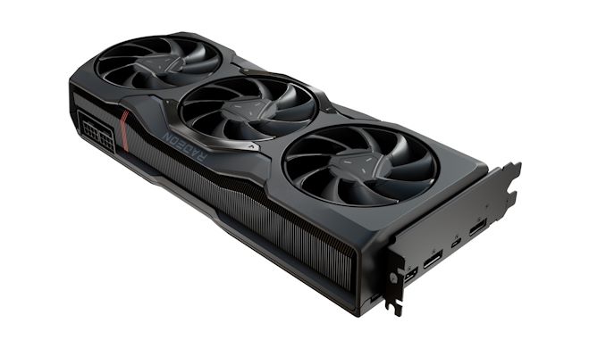
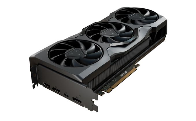
AMD has additionally despatched over footage of each the reference 7900 XTX and 7900 XT. Of specific word, each playing cards will characteristic, for the primary time for an AMD shopper card, a USB-C port for show outputs. Nonetheless not like NVIDIA’s earlier enterprise on this subject, this isn’t for VR use, however as an alternative for extra instantly hooking up displays that depend on DisplayPort Alt Mode over USB-C. Rounding out the gathering might be a paid of DisplayPorts (2.1) and an HDMI 2.1 port.
Each playing cards are utilizing a brand new triple fan blower design from AMD. We’re nonetheless ready on additional particulars right here, however AMD has instructed us that the 7900 XTX measures 287mm lengthy, and is 2.5 slots extensive.
Wrapping issues up, each playing cards might be launching on December 13th, with AMD planning on having each reference and AIB companions’ playing cards on the shelf for launch day. The 7900 XTX will begin at $999, in the meantime the 7900 XT might be proper behind it at $899. AMD isn’t providing any efficiency comparisons versus NVIDIA playing cards, however at this juncture it looks like the wildcard is the soon-to-launch GeForce RTX 4080 16GB. By the point AMD launches in December, we should always have a a lot better concept of the place AMD and NVIDIA’s dueling lineups stand compared to one another.
/cdn.vox-cdn.com/uploads/chorus_asset/file/25385620/247058_Mothers_Day_Gift_Guide_MLouart.jpg)


