
One of many essential deficits Intel has to its competitors in its server platform is core rely – different corporations are enabling extra cores by one among two routes: smaller cores, or particular person chiplets linked collectively. At its Structure Day 2021, Intel has disclosed options about its next-gen Xeon Scalable platform, one among which is the transfer to a tiled structure. Intel is ready to mix 4 tiles/chiplets by way of its quick embedded bridges, main to higher CPU scalability at greater core counts. As a part of the disclosure, Intel additionally expanded on its new Superior Matrix Extension (AMX) expertise, CXL 1.1 help, DDR5, PCIe 5.0, and an Accelerator Interfacing Structure that will result in customized Xeon CPUs sooner or later.
What’s Sapphire Rapids?
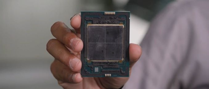
Constructed on an Intel 7 course of, Sapphire Rapids (SPR) will likely be Intel’s next-generation Xeon Scalable server processor for its Eagle Stream platform. Utilizing its newest Golden Cove processor cores which we detailed final week, Sapphire Rapids will convey collectively quite a few key applied sciences for Intel: Acceleration Engines, native half-precision FP16 help, DDR5, 300-Sequence Optane DC Persistent Reminiscence, PCIe 5.0, CXL 1.1, a wider and quicker UPI, its latest bridging expertise (EMIB), new QoS and telemetry, HBM, and workload specialised acceleration.
Set to launch in 2022, Sapphire Rapids will likely be Intel’s first trendy CPU product to reap the benefits of a multi-die structure that goals to attenuate latency and maximize bandwidth as a result of its Embedded Multi-Die Interconnect Bridge expertise. This enables for extra high-performance cores (Intel hasn’t mentioned what number of simply fairly but), with the deal with ‘metrics that matter for its buyer base, comparable to node efficiency and information heart efficiency’. Intel is asking SPR the ‘Greatest Leap in DC Capabilities in a Decade’.
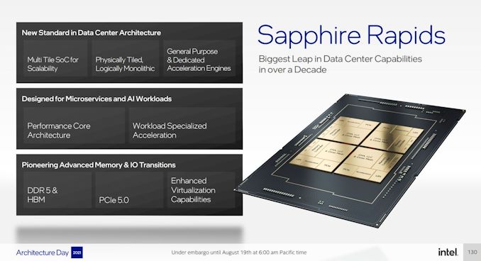
The headline advantages are simple to rattle off. PCIe 5.0 is an improve over the earlier era Ice Lake PCIe 4.0, and we transfer from six 64-bit reminiscence controllers of DDR4 to eight 64-bit reminiscence controllers of DDR5. However the greater enhancements are within the cores, the accelerators, and the packaging.
Golden Cove: A Excessive-Efficiency Core with AMX and AIA
By utilizing the identical core design on its enterprise platform Sapphire Rapids and client platform Alder Lake, there are among the identical synergies we noticed again within the early 2000s when Intel did the identical factor. We coated Golden Cove intimately in our Alder Lake structure deep dive, nonetheless right here’s a fast recap:
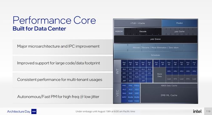
The brand new core, in line with Intel, will over a +19% IPC achieve in single-thread workloads in comparison with Cypress Cove, which was Intel’s backport of Ice Lake. This comes right down to some large core adjustments, together with:
- 16B → 32B size decode
- 4-wide → 6-wide decode
- 5K → 12K department targets
- 2.25K → 4K μop cache
- 5 → 6 huge allocation
- 10 → 12 execution ports
- 352 → 512-entry reorder buffer
The purpose of any core is to course of extra issues quicker, and the most recent era tries to do it higher than earlier than. Plenty of Intel’s adjustments make sense, and people wanting the deeper particulars are inspired to learn our deep dive.
There are some main variations between the patron model of this core in Alder Lake and the server model in Sapphire Rapids. The obvious one is that the patron model doesn’t have AVX-512, whereas SPR can have it enabled. SPR additionally has a 2 MB non-public L2 cache per core, whereas the patron mannequin has 1.25 MB. Past this, we’re speaking about Superior Matrix Extensions (AMX) and a brand new Accelerator Interface Structure (AIA).
To date in Intel’s CPU cores we’ve scalar operation (regular) and vector operation (AVX, AVX2, AVX-512). The following stage up from that could be a devoted matrix solver, or one thing akin to a tensor core in a GPU. That is what AMX does, by including a brand new expandable register file with devoted AMX directions within the type of TMUL directions.
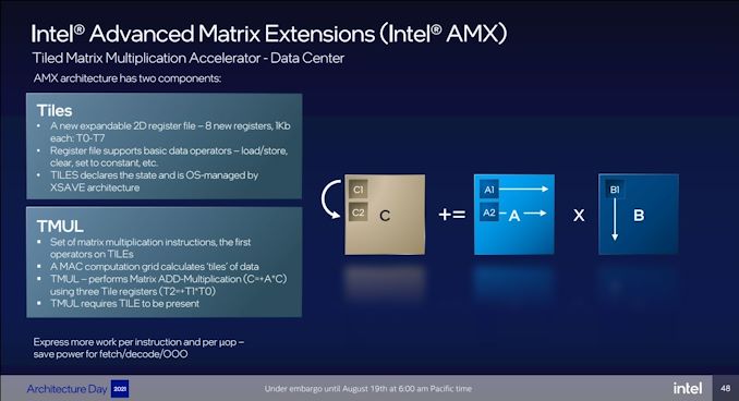
AMX makes use of eight 1024-bit registers for primary information operators, and thru reminiscence references, the TMUL directions will function on tiles of information utilizing these tile registers. The TMUL is supported by way of a devoted Engine Coprocessor constructed into the core (of which every core has one), and the idea behind AMX is that TMUL is just one such co-processor. Intel has designed AMX to be wider-ranging than merely this – within the occasion that Intel goes deeper with its silicon multi-die technique, in some unspecified time in the future we might see customized accelerators being enabled by way of AMX.
Intel confirmed that we shouldn’t see any frequency dips worse than AVX – there are new fine-grained energy controllers per core for when vector and matrix directions are invoked.

This feeds fairly properly into discussing AIA, the brand new accelerator interface. Usually when utilizing add-in accelerator playing cards, instructions should navigate between kernel and person house, arrange reminiscence, and direct any virtualization between a number of hosts. The way in which Intel is describing its new Acceleration Engine interface is akin to speaking to a PCIe system as if it have been merely an accelerator on board to the CPU, despite the fact that it’s hooked up by way of PCIe.
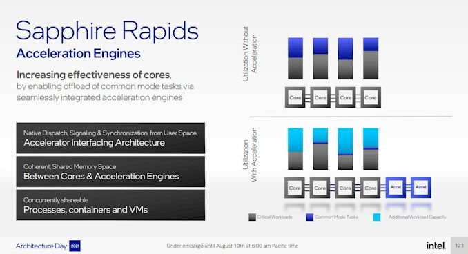
Initially, Intel can have two succesful AIA bits of {hardware}.
Intel Fast Help Know-how (QAT) is one we’ve seen earlier than, because it showcased inside particular variants of Skylake Xeon’s chipset (that required a PCIe 3.0 x16 hyperlink) in addition to an add-in PCIe card – this model will help as much as 400 Gb/s symmetric cryptography, or as much as 160 Gb/s compression plus 160 Gb/s decompression concurrently, double the earlier model.
The opposite is Intel’s Knowledge Streaming Accelerator (DSA). Intel has had documentation about DSA on the internet since 2019, stating that it’s a high-performance information copy and transformation accelerator for streaming information from storage and reminiscence or to different components of the system by way of a DMA remapping {hardware} unit/IOMMU. DSA has been a request from particular hyperscaler prospects, who need to deploy it inside their very own inside cloud infrastructure, and Intel is eager to level out that some prospects will use DSA, some will use Intel’s new Infrastructure Processing Unit, whereas some will use each, relying on what stage of integration or abstraction they’re all for. Intel instructed us that DSA is an improve over the Crystal Seashore DMA engine which was current on the Purley (SKL+CLX) platforms.
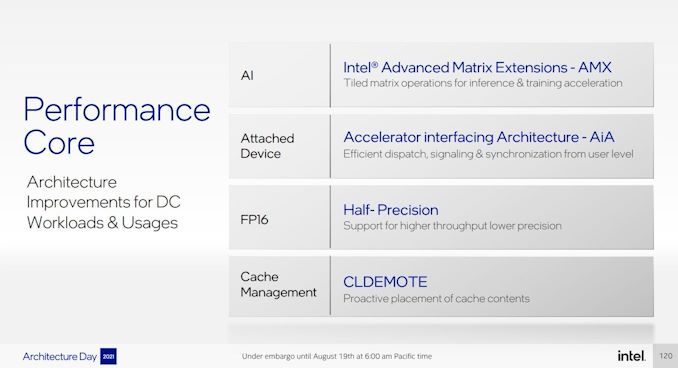
On prime of all this, Sapphire Rapids additionally helps AVX512_FP16 directions for half-precision, principally for AI workloads as a part of its DLBoost technique (Intel was fairly quiet on DLBoost through the occasion). These FP16 instructions will also be used as a part of AMX, alongside INT8 and BF16 help. Intel now additionally helps CLDEMOTE for cache-line administration.
A Facet Phrase about CXL
All through the displays of Sapphire Rapids, Intel has been eager to focus on it would help CXL 1.1 at launch. CXL is a connectivity normal designed to deal with far more than what PCIe does – other than merely appearing as an information switch from host to system, CXL has three branches to help, referred to as IO, Cache, and Reminiscence. As outlined within the CXL 1.0 and 1.1 requirements, these three kind the idea of a brand new method to join a bunch with a tool.
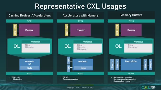
Naturally it was our expectation that every one CXL 1.1 gadgets would help all three of those requirements. It wasn’t till Scorching Chips, a number of days later, that we realized Sapphire Rapids is just supporting a part of the CXL normal, particularly CXL.io and CXL.cache, however CXL.reminiscence wouldn’t be a part of SPR. We’re unsure to what extent this implies SPR is not CXL 1.1 compliant, or what it means for CXL 1.1 gadgets – with out CXL.mem, as per the diagram above, all Intel loses is Kind-2 help. Maybe that is extra of a sign that the market round CXL is healthier served by CXL 2.0, which can little doubt are available a later product.
Within the subsequent web page, we have a look at Intel’s new tiled structure for Sapphire Rapids.


/cdn.vox-cdn.com/uploads/chorus_asset/file/25474031/Crafting_Table_lego.png)
