
Relying in your perspective, the final two years have both passed by very slowly, or in a short time. Whereas the COVID pandemic by no means appeared to finish – and technically nonetheless hasn’t – the final two years have whizzed by for the tech business, and particularly for NVIIDA. The corporate launched its Ampere GPU structure simply two years in the past at GTC 2020, and after promoting extra of their chips than ever earlier than, now in 2022 it’s already time to introduce the subsequent structure. So with out additional ado, let’s discuss in regards to the Hopper structure, which is able to underpin the subsequent era of NVIDIA server GPUs.
As has change into a ritual now for NVIDIA, the corporate is utilizing its Spring GTC occasion to launch its subsequent era GPU structure. Launched simply two years in the past, Ampere has been NVIDIA’s most profitable server GPU structure up to now, with over $10B in information middle gross sales in simply the final 12 months. And but NVIDIA has little time to relaxation on their laurels, because the the expansion and profitability of the server accelerator market signifies that there are extra opponents than ever earlier than aiming take a chunk of NVIDIA’s marketplace for themselves. To that finish, NVIDIA is prepared (and keen) to make use of their greatest present of the 12 months to speak about their subsequent era structure, in addition to the primary merchandise that can implement it.
Taking NVIDIA into the subsequent era of server GPUs is the Hopper structure. Named after pc science pioneer Grace Hopper, the Hopper structure is a really vital, but in addition very NVIDIA replace to the corporate’s ongoing household of GPU architectures. With the corporate’s efforts now solidly bifurcated into server and client GPU configurations, Hopper is NVIDIA doubling down on every thing the corporate does effectively, after which constructing it even larger than ever earlier than.
Hyperbole apart, over the past a number of years NVIDIA has developed a really strong playbook for how one can sort out the server GPU business. On the {hardware} facet of issues that basically boils right down to appropriately figuring out present and future traits in addition to buyer wants in excessive efficiency accelerators, investing within the {hardware} wanted to deal with these workloads at nice speeds, after which optimizing the heck out of all of it. And for NVIDIA, the final step might very effectively be a very powerful bit: NVIDIA places a number of work into getting out of doing work.
That mentality, in flip, is entrance and middle for NVIDIA’s Hopper structure. Whereas NVIDIA has made investments throughout the board to enhance efficiency, from reminiscence bandwidth and I/O to machine studying and confidential computing, the largest efficiency uplifts with Hopper are within the areas the place NVIDIA has found out how one can do much less work, making their processors all of the quicker.
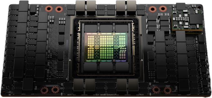
Kicking issues off for the Hopper era is H100, NVIDIA’s flagship server accelerator. Primarily based on the GH100 GPU, GH100 is a standard NVIDIA server-first launch, with the corporate beginning on the excessive finish to develop accelerator playing cards for his or her largest and deepest pocketed server and enterprise prospects.
| NVIDIA Accelerator Specification Comparability | |||||
| H100 | A100 (80GB) | V100 | |||
| FP32 CUDA Cores | 16896 | 6912 | 5120 | ||
| Tensor Cores | 528 | 432 | 640 | ||
| Increase Clock | ~1.78GHz (Not Finalized) |
1.41GHz | 1.53GHz | ||
| Reminiscence Clock | 4.8Gbps HBM3 | 3.2Gbps HBM2e | 1.75Gbps HBM2 | ||
| Reminiscence Bus Width | 5120-bit | 5120-bit | 4096-bit | ||
| Reminiscence Bandwidth | 3TB/sec | 2TB/sec | 900GB/sec | ||
| VRAM | 80GB | 80GB | 16GB/32GB | ||
| FP32 Vector | 60 TFLOPS | 19.5 TFLOPS | 15.7 TFLOPS | ||
| FP64 Vector | 30 TFLOPS | 9.7 TFLOPS (1/2 FP32 fee) |
7.8 TFLOPS (1/2 FP32 fee) |
||
| INT8 Tensor | 2000 TOPS | 624 TOPS | N/A | ||
| FP16 Tensor | 1000 TFLOPS | 312 TFLOPS | 125 TFLOPS | ||
| TF32 Tensor | 500 TFLOPS | 156 TFLOPS | N/A | ||
| FP64 Tensor | 60 TFLOPS | 19.5 TFLOPS | N/A | ||
| Interconnect | NVLink 4 18 Hyperlinks (900GB/sec) |
NVLink 3 12 Hyperlinks (600GB/sec) |
NVLink 2 6 Hyperlinks (300GB/sec) |
||
| GPU | GH100 (814mm2) |
GA100 (826mm2) |
GV100 (815mm2) |
||
| Transistor Depend | 80B | 54.2B | 21.1B | ||
| TDP | 700W | 400W | 300W/350W | ||
| Manufacturing Course of | TSMC 4N | TSMC 7N | TSMC 12nm FFN | ||
| Interface | SXM5 | SXM4 | SXM2/SXM3 | ||
| Structure | Hopper | Ampere | Volta | ||
Forward of at present’s keynote presentation – which as this text goes up, continues to be occurring – NVIDIA supplied a press pre-briefing on Hopper. In conventional NVIDIA style, the corporate has been very selective in regards to the particulars launched so far (least it will get leaked forward of Jensen Huang’s keynote). So we will’t make a completely apples-to-apples comparability to A100 fairly but, as we don’t have the complete specs. However based mostly on this pre-briefing, we will definitely tease out some fascinating highlights about NVIDIA’s structure.
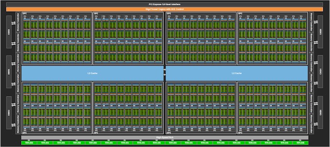
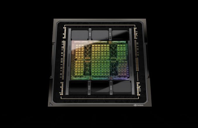
Initially, NVIDIA is as soon as once more constructing massive for his or her flagship GPU. The GH100 GPU is comprised of 80 billion transistors and is being constructed on what NVIDIA is asking a “customized” model of TSMC’s 4N course of node, an up to date model of TSMC’s N5 know-how that provides higher energy/efficiency traits and a really modest enchancment in density. So even at simply two years after Ampere, NVIDIA is making a full node soar after which some for GH100. At this level NVIDIA just isn’t disclosing die sizes, so we don’t have precise figures to share. However given the identified density enhancements of TSMC’s course of nodes, GH100 needs to be shut in measurement to the 826mm2 GA100. And certainly, it’s, at 814mm2.
Like NVIDIA’s earlier sever accelerators, the H100 card isn’t transport with a fully-enabled GPU. So the figures NVIDIA is offering are based mostly on H100 as carried out, with nonetheless many purposeful items (and reminiscence stacks) are enabled.
With regard to efficiency, NVIDIA isn’t quoting any figures for normal vector efficiency upfront. They’re nonetheless quoting tensor efficiency, which relying on the format is both 3x or 6x quicker than the A100 accelerator. We’ll see how this breaks down between clockspeed will increase and both bigger or extra tensor cores, however clearly NVIDIA is as soon as once more throwing much more {hardware} at tensor efficiency, a technique that has labored out effectively for them to this point.
Formally, NVIDIA likes to cite figures with sparsity enabled, however for the needs of our spec sheet I’m utilizing the non-sparse numbers for a extra apples-to-apples comparability with earlier NVIDIA {hardware}, in addition to competing {hardware}. With sparsity enabled, TF32 efficiency and on down might be doubled.
Reminiscence bandwidth can be bettering considerably over the earlier era, with H100 providing 3TB/second of bandwidth there. The rise in bandwidth this time round comes because of using HBM3, with NVIDIA turning into the primary accelerator vendor to make use of the latest-generation model of the excessive bandwidth reminiscence. H100 will include 6 16GB stacks of the reminiscence, with 1 stack disabled. The web result’s 80GB of HBM3 operating at a knowledge fee of 4.8Gbps/pin, and hooked up to a 5120-bit reminiscence bus.
NVIDIA will probably be providing H100 of their ordinary two type elements: SXM mezzanine for prime efficiency servers, and a PCIe card for extra mainstream servers. The ability necessities for each type elements have gone up considerably over the earlier era. NVIDIA is quoting an eye-popping 700 Watt TDP for the SXM model of the cardboard, 75% greater than the official 400W TDP of the A100. For higher or worse, NVIDIA is holding nothing again right here, although the continuing decline in transistor energy scaling just isn’t doing NVIDIA any favors, both.
Cooling such a sizzling GPU will probably be an fascinating job, although not past present know-how. At these energy ranges we’re virtually definitely taking a look at liquid cooling, one thing the SXM type issue is well-suited for. Nonetheless, it’s price noting that the rival OAM type issue – basically the Open Compute Challenge’s tackle SXM to be used in accelerators – is designed to prime out at 700W. So NVIDIA is seemingly approaching the higher limits of what even a mezzanine fashion card can deal with, assuming that sever distributors don’t resort to unique cooling strategies.
In the meantime the H100 PCie card will see its TDP raised to 350W, from 300W at present. Provided that 300W is the normal restrict for PCIe playing cards, will probably be fascinating to see how NVIDIA and their companions hold these playing cards cool. In any other case, with simply half the TDP of the SXM card, we’re anticipating the PCIe model to be clocked/configured noticeably slower in an effort to mood the cardboard’s energy consumption.
Hopper Tensor Cores: Now With Transformer Engines
Transferring on to the big-ticket architectural options of the Hopper structure, we’re begin with NVIDIA’s Transformer Engines. Dwelling as much as their identify, the transformer engines are a brand new, extremely specialised kind of tensor core, which can be designed to additional speed up transformer ML fashions.
In line with NVIDIA’s deal with machine studying, for the Hopper structure the corporate has taken a contemporary take a look at the make-up of the ML market, and what workloads are fashionable and/or essentially the most demanding on current {hardware}. The winner, on this regard, has been transformers, a sort of deep studying mannequin which have risen in reputation quite shortly attributable to their utility in pure language processing and pc imaginative and prescient. Current developments in transformer know-how, such because the GPT-3 mannequin, together with demand from service operators for higher pure language processing, have made transformers the most recent massive breakthrough in ML.
However on the identical time, the processing necessities for transformers are additionally hampering the event of even higher fashions. In brief, higher fashions require an ever-larger variety of parameters, and at over 175 billion parameters for GPT-3 alone, coaching instances for transformers have gotten unwieldy, even on giant GPU clusters.
To that finish, NVIDIA has developed a variant of the tensor core particularly for rushing up transformer coaching and inference, which they’ve dubbed the Transformer Engine. NVIDIA has optimized this new unit by stripping it down to simply processing the decrease precision information codecs utilized by most transformers (FP16), after which scaling issues down much more with the introduction of an FP8 format as effectively. The purpose with the brand new items, in short, is to make use of the minimal precision needed at each step to coach transformers with out shedding accuracy. In different phrases, to keep away from doing extra work than is critical.
![]()
With that mentioned, in contrast to extra conventional neural community fashions that are skilled at a set precision all through, NVIDIA’s newest hack for transformers is to differ the precision, since FP8 can’t be used all through a mannequin. In consequence, Hopper’s transformer engines can swap between FP16 and FP8 coaching on a layer by layer foundation, using NVIDIA-provided heuristics that work to pick the bottom precision wanted. The web profit is that each layer that may be processed at FP8 might be processed twice as quick, because the transformer engines can pack and course of FP8 information twice as shortly as FP16.
Mixed with the extra reminiscence on H100 and the quicker NVLink 4 I/O, and NVIDIA claims that a big cluster of GPUs can prepare a transformer as much as 9x quicker, which might convey down coaching instances on at present’s largest fashions right down to a extra affordable time period, and make even bigger fashions extra sensible to sort out.
In the meantime, on the inference facet of issues, Hopper may also instantly devour its personal FP8 skilled fashions for inference use. This is a vital distinction for Hopper, because it permits prospects to in any other case skip changing and optimizing a skilled transformer mannequin right down to INT8. NVIDIA isn’t claiming any particular efficiency advantages from sticking with FP8 over INT8, but it surely means builders can get pleasure from the identical efficiency and reminiscence utilization advantages of operating inference on an INT8 mannequin with out the previously-required conversion step.
Lastly, NVIDIA is claiming wherever between a 16x and 30x improve in transformer inference efficiency on H100 versus A100. Like their coaching claims, that is an H100 cluster versus an A100 cluster, so reminiscence and I/O enhancements are additionally enjoying an element right here, but it surely none the much less underscores that H100’s transformer engines aren’t only for rushing up coaching.
DPX Directions: Dynamic Programming for GPUs
NVIDIA’s different massive smart-and-lazy enchancment for the Hopper structure comes courtesy of the sector of dynamic programming. For his or her newest era of know-how, NVIDIA is including help for the programming mannequin by including a brand new set of directions only for dynamic programming. The corporate is asking these DPX Directions.
Dynamic programming, in a nutshell, is a method of breaking down advanced issues into smaller, less complicated issues in a recursive method, after which fixing these smaller issues first. The important thing characteristic of dynamic programming is that if a few of these sub-problems are an identical, then these redundancies might be recognized and eradicated – that means a sub-problem might be solved as soon as, and its outcomes saved for future use inside the bigger downside.
All of which is to say that, like Sparsity and Transformer Engines, NVIDIA is implementing dynamic programming to permit their GPUs to get out of doing extra work. By eliminating the redundant elements of workloads that may be damaged up per the principles of dynamic programming, it’s that a lot much less work NVIDIA’s GPUs have to do, and that a lot quicker they’ll produce outcomes.
Although in contrast to Transformer Engines, including dynamic programming help through the DPX Directions just isn’t a lot about rushing up current workloads on GPUs as it’s enabling new workloads on GPUs. Hopper is the primary NVIDIA structure to help dynamic programming, so workloads that may be resolved with dynamic programming are usually run on CPUs and FPGAs. In that respect, that is NVIDIA discovering yet another workload they’ll steal from CPUs and run on a GPU as an alternative.
General, NVIDIA is claiming a 7x enchancment in dynamic programming algorithm efficiency on a single H100 versus naïve execution on an A100.
As for the real-world implications of DPX Directions, NVIDIA is citing route planning, information science, robotics, and biology as all being potential beneficiaries of the brand new know-how. These fields already use a number of well-known dynamic programming algorithms, akin to Smith-Waterman and Flyod-Warshall, which rating genetic sequence aligning and discover the shortest distances between pairs of locations respectively.
General, dynamic programming is among the extra area of interest fields amongst excessive efficiency workloads. But it surely’s one which NVIDIA believes generally is a good match for GPUs as soon as the proper {hardware} help is accessible.
Confidential Computing: Defending GPU Knowledge From Prying Eyes
Shifting away from performance-focused options, NVIDIA’s different massive push with the Hopper structure is on the safety entrance. With the growth of GPU utilization in cloud computing environments – and particularly shared VM environments – the corporate is taking a brand new deal with the safety issues that entails, and how one can safe shared programs.
The top results of these efforts is that Hopper is introducing {hardware} help for trusted execution environments. Particularly, Hopper helps the creation of what NVIDIA is terming a confidential digital machine, the place all the information inside the VM setting is safe, and all the information getting into (and leaving) the setting is encrypted.
NVIDIA didn’t go over too lots of the technical particulars underpinning their new security measures in our-pre-briefing, however in line with the corporate it’s a product of a mixture of new {hardware} and software program options. Of specific word, information encryption/decryption when shifting to and from the GPU is quick sufficient to be executed on the PCIe line fee (64GB/sec), that means there’s no slowdown by way of sensible host-to-GPU bandwidth when utilizing this safety characteristic.
This trusted execution setting, in flip, is designed to withstand all types of tampering. The reminiscence contents inside the GPU itself are secured by what NVIDIA is terming a “{hardware} firewall”, which prevents exterior processes from touching them, and this identical safety is prolonged to information in-flight within the SMs as effectively. The trusted setting can be mentioned to be secured in opposition to the OS or the hypervisor accessing the contents of the GPU from above, limiting entry to simply the proprietor of the VM. Which is to say that, even with bodily entry to the GPU, it shouldn’t be doable to entry the information inside a safe VM on hopper.
In the end, NVIDIA’s goal right here seems to be making/maintaining their prospects comfy utilizing GPUs to course of delicate information by making them a lot {hardware} to interrupt into after they’re working in a secured mode. This, in flip, just isn’t solely to guard historically delicate information, akin to medical information, but in addition to guard the type of high-value AI fashions that a few of NVIDIA’s prospects are actually creating. Given all the work that may go into creating and coaching a mannequin, prospects don’t need their fashions getting copied, be it in a shared cloud setting or being pulled out of a bodily insecure edge gadget.
Multi-Occasion GPU v2: Now With Isolation
As an extension of NVIDIA’s safety efforts with confidential computing, the corporate has additionally prolonged these protections to their Multi-Occasion GPU (MIG) setting. MIG cases can now be totally remoted, with I/O between the occasion and the host totally virtualized and secured as effectively, basically granting MIG cases the identical security measures as H100 general. General, this strikes MIG nearer to CPU virtualization environments, the place the assorted VMs assume to not belief one another and are stored remoted.
NVLink 4: Extending Chip I/O Bandwidth to 900GB/sec
With the Hopper structure additionally comes a brand new rendition of NVIDIA’s NVLink high-bandwidth interconnect for wiring up GPUs (and shortly, CPUs) collectively for higher efficiency in workloads that may scale out over a number of GPUs. NVIDIA has iterated on NVLink with each era of their flagship GPU, and this time isn’t any completely different, with the introduction of NVLink 4.
Whereas we’re awaiting a full disclosure of technical specs from NVIDIA, the corporate has confirmed that NVLink bandwidth on a per-chip foundation has been elevated from 600GB/second on A100 to 900GB/second for H100. Be aware that that is the sum complete of all upstream and downstream bandwidth throughout all the particular person hyperlinks that NVLink helps, so lower these figures in half to get particular transmit/obtain charges.
| NVLink Specification Comparability | |||||
| NVLink 4 | NVLink 3 | NVLink 2 | |||
| Signaling Charge | 100 Gbps | 50 Gbps | 25 Gbps | ||
| Lanes/Hyperlink | 2 | 4 | 8 | ||
| Bandwidth/Course/Hyperlink | 25 GB/sec | 25 GB/sec | 25 GB/sec | ||
| Complete Bandwidth/Hyperlink | 50 GB/sec | 50 GB/sec | 50 GB/sec | ||
| Hyperlinks/Chip | 18 (GH100) |
12 (GA100) |
6 (GV100) |
||
| Bandwidth/Chip | 900 GB/sec | 600 GB/sec | 300 GB/sec | ||
900GB/sec represents a 50% improve in I/O bandwidth for H100. Which isn’t as nice a rise as H100’s complete processing throughput, however a practical enchancment given the ever-escalating complexities in implementing quicker networking charges.
Provided that NVLink 3 was already operating at a 50 Gbit/sec signaling fee, it’s not clear if the extra bandwidth is courtesy of an excellent quicker signaling fee, or if NVIDIA has as soon as once more adjusted the variety of hyperlinks coming from the GPU. NVIDIA beforehand altered the NVLink lane configuration for A100, after they halved the lane width and doubled the variety of lanes, all whereas doubling the signaling fee. Including lanes on prime of meaning not having to determine how one can enhance the signaling fee by much more, but it surely additionally means a 50% improve within the variety of pins wanted for NVLink I/O.
Alongside these traces, it’s additionally price noting that NVIDIA is including PCIe 5.0 help with Hopper. As PCIe continues to be used for host-to-GPU communications (till Grace is prepared, at the very least), this implies NVIDIA has doubled their CPU-GPU bandwidth, letting them hold H100 that significantly better fed. Although placing PCIe 5.0 to good use goes to require a bunch CPU with PCIe 5.0 help, which isn’t one thing AMD or Intel are offering fairly but. Presumably, somebody could have {hardware} prepared and transport by the point NVIDIA ships H100 in Q3, particularly since NVIDIA is keen on homogenization for his or her DGX pre-built servers.
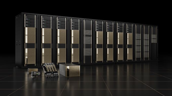
Lastly, with the launch of H100/NVLink 4, NVIDIA can be utilizing this time to announce a brand new, exterior NVLink swap. This exterior swap extends past NVIDIA’s present on-board NVSwitch performance, which is used to assist construct extra advanced GPU topologies inside a single node, and permits H100 GPUs to instantly talk with one another throughout a number of nodes. In essence, it’s a alternative for having NVIDIA GPUs undergo Infiniband networks in an effort to talk cross-node.
The exterior NVLInk Swap permits for as much as 256 GPUs to be related collectively inside a single area, which works out to 32 8-way GPU nodes. In line with NVIDIA, a single, 1U NVLink Swap presents 128 lanes of NVLink through 32 Octal SFP (OSFP) transceivers. The total Swap, in flip, presents a complete bisection bandwidth of 70.4TB/second.
It’s price noting, nonetheless, that the NVLink Swap just isn’t a wholesale alternative for Infiniband – which after all, NVIDIA additionally sells via its networking {hardware} division. Infiniband connections between nodes are nonetheless wanted for different kinds of communications (e.g. CPU to CPU), so exterior NVLink networks are a complement to Infiniband, permitting H100 GPUs to instantly chat amongst themselves.
NVIDIA HGX Rides Once more: HGX For H100
Final, however not least, NVIDIA has confirmed that they’re updating their HGX baseboard ecosystem for H100 as effectively. A staple of NVIDIA’s multi-GPU designs since they first started utilizing the SXM type issue for GPUs, HGX baseboards are NVIDIA-produced GPU baseboards for system builders to make use of in designing full multi-GPU programs. The HGX boards present the complete connection and mounting setting for NVIDIA’s SXM type issue GPUs, after which sever distributors can route energy and PCIe information (amongst different issues) from their motherboards to the HGX baseboard. For the present A100 era, NVIDIA has been promoting 4-way, 8-way, and 16-way designs.
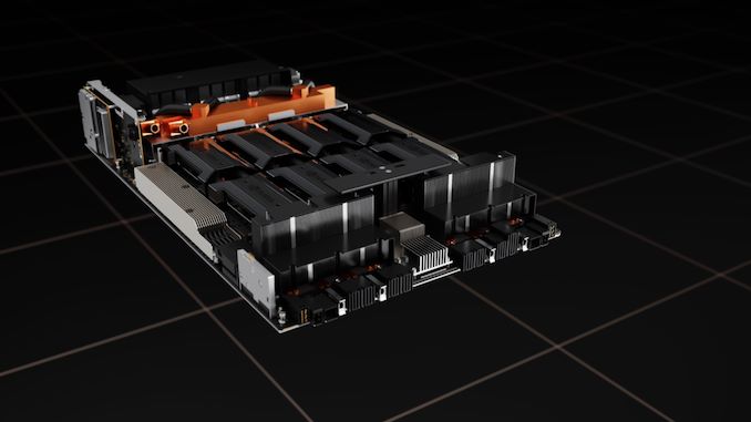
Relative to the GPUs themselves, HGX is quite unexciting. But it surely’s an vital a part of NVIDIA’s ecosystem. Server companions can pickup an HGX board and GPUs, after which shortly combine that right into a server design, quite than having to design their very own server from scratch. Which within the case of H100, signifies that establishment will (largely) reign, and that NVIDIA’s server companions will be capable of assemble programs in the identical method as earlier than.
Hopper H100 Accelerators: Delivery In Q3 2022
Wrapping issues up, NVIDIA is planning on having H100-equipped programs accessible in Q3 of this 12 months. This can embody NVIDIA’s full suite of self-built programs, together with DGX and DGX SuperPod servers, in addition to servers from OEM companions utilizing HGX baseboards and PCIe playing cards. Although in typical style, NVIDIA just isn’t saying particular person H100 pricing, citing the truth that they promote this {hardware} via server companions. We’ll have a bit extra perception as soon as NVIDIA proclaims the costs of their very own DGX programs, however suffice it to say, don’t count on H100 playing cards to return low-cost.


/cdn.vox-cdn.com/uploads/chorus_asset/file/25430225/247065_Vergecast_Gaming_Senses_Smell_SHaddad.png)
