
This week we have now the annual Supercomputing occasion the place all the main Excessive Efficiency Computing gamers are placing their playing cards on the desk in terms of {hardware}, installations, and design wins. As a part of the occasion Intel is having a presentation on its {hardware} choices, which discloses further particulars in regards to the subsequent technology {hardware} going into the Aurora Exascale supercomputer.
Aurora is a contract that Intel has had for a while – the scope was initially to have a 10nm Xeon Phi based mostly system, for which the thought was mothballed when Xeon Phi was scrapped, and has been an ever altering panorama because of Intel’s {hardware} choices. It was finalized a few years in the past that the system would now be utilizing Intel’s Sapphire Rapids processors (those that include Excessive Bandwidth Reminiscence) mixed with new Ponte Vecchio Xe-HPC based mostly GPU accelerators and boosted from a number of hundred PetaFLOPs to an ExaFLOP of compute. Most lately, Intel CEO Pat Gelsinger has disclosed that the Ponte Vecchio accelerator is attaining double the efficiency, above the expectations of the unique disclosures, and that Aurora will probably be a 2+EF Supercomputer when constructed. Intel is anticipating to ship the primary batch of {hardware} to the Argonne Nationwide Laboratory by the tip of the 12 months, however this may include $300m write-off on Intel’s This fall financials. Intel is anticipating to ship the remainder of the machine by way of 2022 in addition to ramp up the manufacturing of the {hardware} for mainstream use by way of Q1 for wider unfold launch within the first half of the 12 months.
In the present day we have now further particulars in regards to the {hardware}.
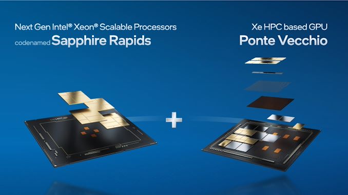
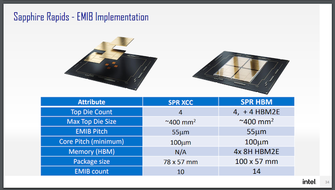
On the processor facet, we all know that every unit of Aurora will characteristic two of Intel’s latest Sapphire Rapids CPUs (SPR), that includes 4 compute tiles, DDR5, PCIe 5.0, CXL 1.1 (not CXL.mem), and will probably be liberally utilizing EMIB connectivity between the tiles. Aurora can even be utilizing SPR with built-in Excessive Bandwidth Reminiscence (SPR+HBM), and the primary disclosure is that SPR+HBM will provide as much as 64 GB of HBM2e utilizing 8-Hello stacks.
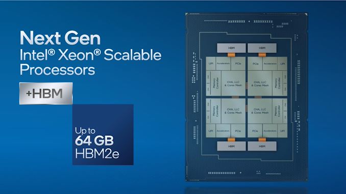
Primarily based on the representations, Intel intends to make use of 4 stacks of 16 GB HBM2e for a complete of 64 GB. Intel has a relationship with Micron, and the Micron HBM2e bodily dimensions are consistent with the representations given in Intel’s supplies (in comparison with say, Samsung or SKHynix). Micron at the moment affords two variations of 16 GB HBM2E with ECC {hardware}: one at 2.8 Gbps per pin (358 GB/s per stack) and one at 3.2 Gbps per pin (410 GB/s per stack). Total we’re a peak bandwidth then between 1.432 TB/s to 1.640 TB/s relying on which model Intel is utilizing. Variations with HBM will use a further 4 tiles, to attach every HBM stack to one among SPR’s chiplets.
Primarily based on this diagram from Intel, regardless of Intel stating that SPR+HBM will share a socket with conventional SPR, it’s clear that there will probably be variations that aren’t suitable. This can be an occasion the place the Aurora variations of SPR+HBM are tuned particularly for that machine.
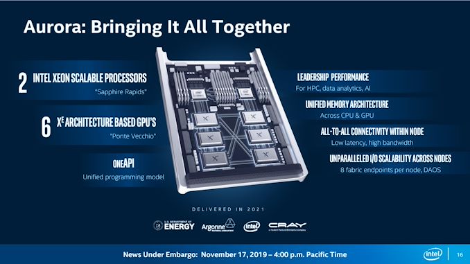
On the Ponte Vecchio (PVC) facet of the equation, Intel has already disclosed {that a} single server inside Aurora could have six PVC accelerators per two SPR processors. Every of the accelerators will probably be related in an all-to-all topology to one another utilizing the brand new Xe-Hyperlink protocol constructed into every PVC – Xe-Hyperlink helps 8 in totally related mode, so Aurora solely needing six of these saves extra energy for the {hardware}. It’s not been disclosed how they’re related to the SPR processors – Intel has said that there will probably be a unified reminiscence structure between CPU and GPU.
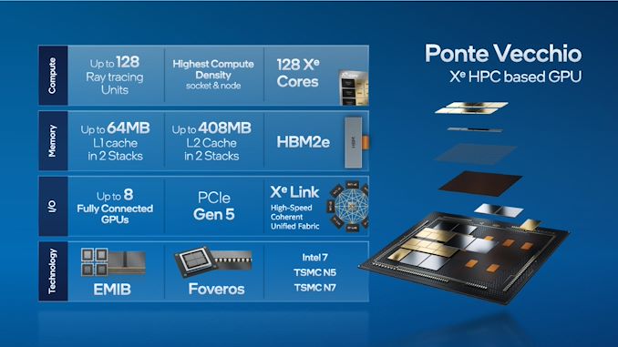
The perception added in the present day by Intel is that every Ponte Vecchio dual-stack implementation (the diagram Intel has proven repeatedly is 2 stacks facet by facet) will characteristic a complete of 64 MB of L1 cache and 408 MB of L2 cache, backed by HBM2e.
408 MB of L2 cache throughout two stacks means 204 MB per stack. If we examine that to different {hardware}:
- NVIDIA A100 has 40 MB of L2 cache
- AMD’s Navi 21 has 128 MB of Infinity Cache (an efficient L3)
- AMD’s CNDA2 MI250X in Frontier has 8 MB of L2 per ‘stack’, or 16 MB whole
Whichever means you slice it, Intel is betting arduous on having the proper hierarchy of cache for PVC. Diagrams of PVC additionally present 4 HBM2e chips per half, which suggests that every PVC dual-stack design might need 128 GB of HBM2e. It’s probably that none of them are ‘spare’ for yield functions, as a chiplet based mostly design permits Intel to construct PVC utilizing identified good die from the start.
On prime of this, we additionally get an official quantity as to the dimensions of what number of Ponte Vecchio GPUs and Sapphire Rapids (+HBM) processors we’d like for Aurora. Again in November 2019, when Aurora was solely listed as a 1EF supercomputer, I crunched some tough numbers based mostly on Intel saying Aurora was 200 racks and making educated guesses on the structure – I bought to 5000 CPUs and 15000 GPUs, with every PVC needing round 66.6TF of efficiency. On the time, Intel was already exhibiting off 40 TF of efficiency per card on early silicon. Intel’s official numbers for the Aurora 2EF machine are:
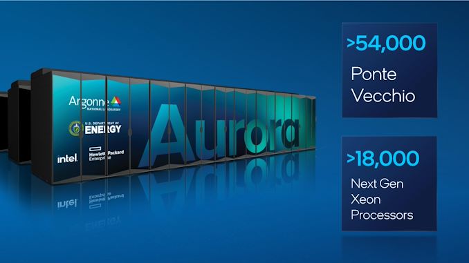
18000+ CPUs and 54000+ GPUs is a number of {hardware}. However dividing 2 Exaflops by 54000 PVC accelerators involves solely 37 TeraFlops per PVC as an higher certain, and that quantity is assuming zero efficiency is coming from the CPUs.
So as to add into the combo: Intel CEO Pat Gelsinger solely a few weeks in the past mentioned that PVC was coming in at double the efficiency initially anticipated, permitting Aurora to be a 2EF machine. Does that imply the unique efficiency goal for PVC was ~20 TF of FP64? Apropos of nothing, AMD’s current MI250X announcement final week showcased a dual-GPU chip with 47.9 TF of FP64 vector efficiency, transferring to 95.7 TF in FP64 matrix efficiency. The tip consequence right here may be that AMD’s MI250X is definitely greater uncooked efficiency than PVC, nonetheless AMD requires 560 W for that card, whereas Intel’s energy numbers haven’t been disclosed. We might do some serviette math right here as properly.
- Frontier makes use of 560 W MI250X playing cards, and is rated for 1.5 ExaFlops of FP64 Vector at 30 MW of energy. This implies Frontier wants 31300 playing cards (1.5 EF / 49.7 TF) to satisfy efficiency targets, and for every 560 W MI250X card, Frontier has allotted 958 Watts of energy (30 MW / 31300 playing cards). It is a 71% overhead for every card (which implies cooling, storage methods, different compute/administration and so forth).
- Aurora makes use of PVC at an unknown energy, is rated for two ExaFlops of FP64 Vector at 60 MW of energy. We all know that PVC has 54000+ playing cards to satisfy efficiency targets, which implies that the system has allotted 1053 W (that’s 60 MW / 54000) per card to incorporate the PVC accelerator and different overheads required. If we have been to imagine (a giant assumption I do know) that Frontier and Aurora have related overheads, then we’re 615 W per PVC.
- This is able to find yourself with PVC at 615 W for 37 TF, towards MI250X at 560 W for 47.9 TF.
- This uncooked dialogue fails to debate particular options every card has for its use case.
| Compute GPU Accelerator Comparability Confirmed Numbers |
|||
| AnandTech | Intel | AMD | NVIDIA |
| Product | Ponte Vecchio | MI250X | A100 80GB |
| Structure | Xe-HPC | CDNA2 | Ampere |
| Transistors | 100 B | 58.2 B | 54.2 B |
| Tiles (inc HBM) | 47 | 10 | 6 + 1 spare |
| Compute Models | 128 | 2 x 110 | 108 |
| Matrix Cores | 128 | 2 x 440 | 432 |
| INT8 Tensor | ? | 383 TOPs | 624 TOPs |
| FP16 Matrix | ? | 383 TOPs | 312 TOPs |
| FP64 Vector | ? | 47.9 TFLOPS | 9.5 TFLOPS |
| FP64 Matrix | ? | 95.7 TFLOPs | 19.5 TFLOPS |
| L2 / L3 | 2 x 204 MB | 2 x 8 MB | 40 MB |
| VRAM Capability | 128 GB (?) | 128 GB | 80 GB |
| VRAM Sort | 8 x HBM2e | 8 x HBM2e | 5 x HBM2e |
| VRAM Width | ? | 8192-bit | 5120-bit |
| VRAM Bandwidth | ? | 3.2 TB/s | 2.0 TB/s |
| Chip-to-Chip Whole BW | 8 | 8 x 100 GB/s | 12 x 50 GB/s |
| CPU Coherency | Sure | With IF | With NVLink 3 |
| Manufacturing | Intel 7 TSMC N7 TSMC N5 |
TSMC N6 | TSMC N7 |
| Kind Components | OAM | OAM (560 W) | SXM4 (400W*) PCIe (300W) |
| Launch Date | 2022 | 11/2021 | 11/2020 |
| *Some Customized deployments go as much as 600W | |||
Intel additionally disclosed that will probably be partnering with SiPearl to deploy PVC {hardware} within the European HPC efforts. SiPearl is at the moment constructing an Arm-based CPU known as Rhea constructed on TSMC N7.
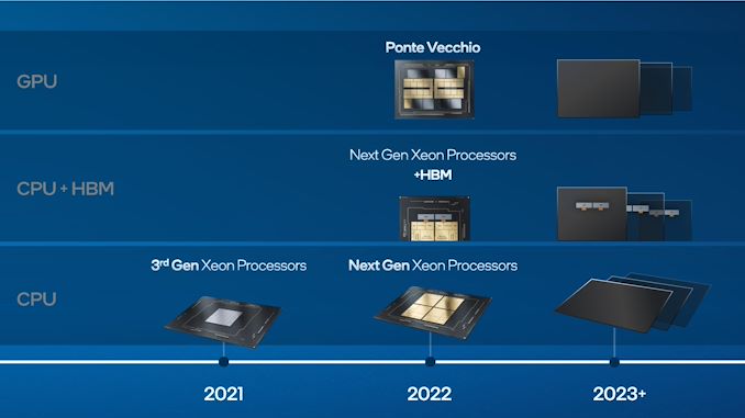
Transferring ahead, Intel additionally launched a mini-roadmap. Nothing too stunning right here – Intel has plans for designs past Ponte Vecchio, and that future Xeon Scalable processors can even have choices enabled with HBM.
Associated Studying


