
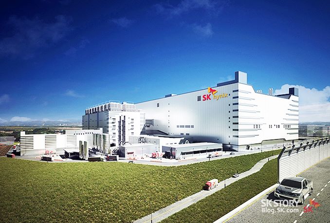
SK hynix this week introduced plans to construct its superior reminiscence packaging facility in West Lafayette, Indiana. The transfer will be thought-about as a milestone each for the reminiscence maker and the U.S., as that is the primary superior reminiscence packaging facility within the nation and the corporate’s first important manufacturing operation in America. The ability shall be used to construct next-generation kinds of high-bandwidth reminiscence (HBM) stacks when it begins operations in 2028. Additionally, SK hynix agreed to work on R&D initiatives with Purdue College.
“We’re excited to change into the primary within the trade to construct a state-of-the-art superior packaging facility for AI merchandise in america that may assist strengthen supply-chain resilience and develop an area semiconductor ecosystem,” mentioned SK hynix CEO Kwak Noh-Jung.
One in all The Most Superior Chip Packaging Facility Ever
The ability will deal with meeting of HBM recognized good stacked dies (KGSDs), which encompass a number of reminiscence units stacked on a base die. Moreover, it will likely be used to develop next-generations of HBM and can subsequently home a packaging R&D line. Nonetheless, the plant is not going to make DRAM dies themselves, and can possible supply them from SK hynix’s fabs in South Korea.
The plant would require SK hynix to speculate $3.87 billion, which can make it one of the crucial superior semiconductor packaging services on the planet. In the meantime, SK hynix held the funding settlement ceremony with representatives from Indiana State, Purdue College, and the U.S. authorities, which signifies events financially concerned within the venture, however this week’s occasion didn’t disclose whether or not SK hynix will obtain any cash from the U.S. authorities underneath the CHIPS Act or different funding initiatives.
The price of the power considerably exceeds that of packaging services constructed by different main gamers within the trade, akin to ASE Group, Intel, and TSMC, which highlights how important of an funding that is for SK hnix. In actual fact, $3.87 billion increased than superior packaging CapEx budgets of Intel, TSMC and Samsung in 2023, primarily based on estimates from Yole Intelligence.
On condition that the fab comes on-line in 2028, primarily based on SK hynix’s product roadmap we would anticipate that it will likely be used at the very least partly to assemble HBM4 and HBM4E stacks. Notably, since HBM4 and HBM4E stacks are set to function a 2048-bit interface, their packaging course of shall be significantly extra advanced than the prevailing 1024-bit HBM3/HBM3E packaging and would require utilization of extra superior instruments, which is why it’s poised to be costlier than some current superior packaging services. Because of the extraordinarily advanced 2048-bit interface, many chip designers who’re going to make use of HBM4/HBM4E are anticipated to combine it immediately onto their processors utilizing hybrid bonding and never use silicon interposers. Sadly, it’s unclear whether or not the SK hynix facility will be capable of provide such service.
HBM is especially used for AI and HPC purposes, so it’s strategically vital to have its manufacturing within the U.S. In the meantime, precise reminiscence dies will nonetheless must be made elsewhere, at devoted DRAM fabs.
Purdue College Collaboration
Along with assist set to be supplied by state and native governmens, SK hynix selected to ascertain its new facility in West Lafayette, Indiana, to collaborate with Purdue College in addition to with Purdue’s Birck Nanotechnology Middle on R&D initiatives, which incorporates superior packaging and heterogeneous integration.
SK hynix intends to work in partnership with Purdue College and Ivy Tech Neighborhood School to create coaching applications and multidisciplinary diploma programs geared toward nurturing a talented workforce and establishing a constant stream of rising expertise for its superior reminiscence packaging facility and R&D operations.
“SK hynix is the worldwide pioneer and dominant market chief in reminiscence chips for AI,” Purdue College President Mung Chiang mentioned. “This transformational funding displays our state and college’s super energy in semiconductors, {hardware} AI, and exhausting tech hall. Additionally it is a monumental second for finishing the availability chain of digital economic system in our nation by way of chips superior packaging. Situated at Purdue Analysis Park, the biggest facility of its sort at a U.S. college will develop and succeed by way of innovation.”

/cdn.vox-cdn.com/uploads/chorus_asset/file/25430170/203746_thermostats_ecobee_ebstat02.jpeg)

