
At present nearly all of high-end processors are monolithic, however design methodologies are slowly however certainly shifting to multi-chiplet modules as modern fabrication applied sciences get costlier to make use of. Within the coming years multi-chiplet system-in-packages (SiPs) are anticipated to develop into rather more widespread, and superior 2.5D and 3D chip packaging applied sciences will achieve significance. To speed up and simplify improvement of 3D designs, TSMC this week established its 3DFabric Alliance.
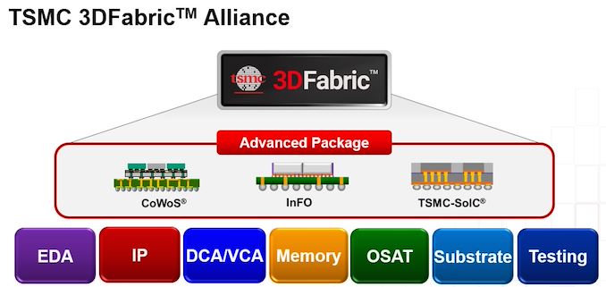
Whereas multi-chiplet SiPs promise to simplify improvement and verification of extremely complicated designs, they require brand-new improvement methodologies as 3D packages carry various new challenges. This consists of new design flows required for 3D integration, new strategies of energy supply, new packaging applied sciences, and new testing methods. To make the perfect use of the advantages of TSMC’s 2.5D and 3D packaging applied sciences (InFO, CoWoS, and SoIC), the chip improvement trade wants the entire ecosystem to work in live performance on chiplet packaging – and that is what 3DFabric Alliance is designed to do.
“3D silicon stacking and superior packaging applied sciences open the door to a brand new period of chip-level and system-level innovation, and likewise require intensive ecosystem collaboration to assist designers navigate the perfect path by means of the myriad choices and approaches obtainable to them,” stated Dr. L.C. Lu, TSMC fellow and vice chairman of design and expertise platform.
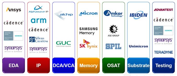
TSMC’s 3DFabric Alliance brings collectively builders of digital design automation (EDA) instruments, mental property suppliers, contract chip designers, reminiscence producers, superior substrate producers, semiconductor meeting and check firms, and the teams making the gear used for testing and verification. The alliance at present has 19 members, however over time it’s anticipated to increase as new members be a part of the group.
Because the chief of the Alliance, TSMC will set sure floor guidelines and requirements. In the meantime members of 3DFabric Alliance will co-define and co-develop a few of the specs for TSMC’s 3DFabric applied sciences, will achieve early entry to TSMC’s 3DFabric roadmap and specs to align their plans with the foundry’s plans in addition to these of different members of the alliance, and can have the ability to design and optimize options which are appropriate with the brand new packaging strategies.
Finally, TSMC needs to make sure that members of 3DFabric Alliance will supply its shoppers appropriate and interoperable options that may allow fast improvement and verification of multi-chiplet SiPs that use 2.5D and 3D packaging.
For instance, to unify the design ecosystem with certified EDA instruments and flows, TSMC has developed its 3Dblox normal. 3Dblox covers varied elements of constructing multi-chiplet units that includes 2.5D and 3D packaging methodologies (equivalent to chiplet and interface definitions), together with bodily implementation, energy consumption, warmth dissipation, electro-migration IR drop (EMIR), and timing/bodily verification.
“By way of the collective management of TSMC and our ecosystem companions, our 3DFabric Alliance provides prospects a simple and versatile method to unlocking the ability of 3D IC of their designs, and we will’t wait to see the improvements they’ll create with our 3DFabric applied sciences,” added Lu.
Finally, TSMC envisions that the alliance will enormously simplify and streamline the method for growing extra superior chips, particularly for small and mid-size firms that rely extra closely on outdoors IP/designs. For instance, if an organization needs to develop a SiP consisting of logic chiplets stacked collectively and related to an HBM3-based reminiscence subsystem, EDA software program from Ansys Cadence, Synopsys, and Siemens will permit it to design appropriate chiplets, IP suppliers will promote these blocks the designer doesn’t have already got, TSMC will produce silicon, reminiscence producers will supply appropriate HBM3 KGSDs (recognized good stack dies), after which Ase Expertise will assemble all the things collectively. In the meantime firms that would not have their very own engineers will have the ability to order the design of the entire SiP (or particular person chiplets) by means of Alchip or GUC, after which replace their product over time if wanted with no need to revamp all the things, because the SiP will probably be in-built accordance with 3DFabric and 3Dblox requirements.
3Dblox is at present supported by 4 main EDA builders. Finally will probably be supported by all members of the members if the alliance the place wanted.
Whereas giant firms like AMD and Nvidia are likely to develop their very own IP, interconnection, and packaging applied sciences, multi-chiplet SiPs promise to make the event of complicated, chiplet-style processors accessible to smaller firms. For them, normal third-party IP, quick time-to-market, and correct integration are key to success, so 3DFabric Alliance and what it brings will probably be important for them.
Supply: TSMC


